Clock signal duty ratio adjusting circuit
A clock signal and regulating circuit technology, applied in the direction of electrical components, electric pulse generation, pulse generation, etc., can solve the problem of clock signal instability and achieve the effect of avoiding the instability of the output clock signal
- Summary
- Abstract
- Description
- Claims
- Application Information
AI Technical Summary
Problems solved by technology
Method used
Image
Examples
Embodiment Construction
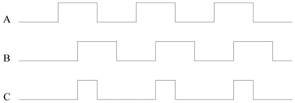
[0024] refer to figure 1 The timing diagram, A represents the waveform of the clock signal with a duty ratio of 50% generated by the clock generation circuit, B represents the waveform of the clock signal with a duty ratio of 50% after the delay circuit, and C represents A and B The waveform after passing through the AND gate circuit can generate a clock signal with a duty ratio of 25%. However, although the above solution is relatively easy to implement, there are large errors because the parameters of the delay circuit itself will change with changes in process, temperature, voltage and other environmental factors.
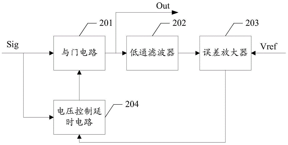
[0025] In order to overcome the above-mentioned problems, another clock duty ratio adjustment method appears. refer to figure 2 , including: an AND gate circuit 201 , a low-pass filter 202 , an error amplifier 203 and a voltage-controlled delay circuit 204 . The AND gate circuit 201 performs an AND operation on the clock signal Sig with a duty cycle of 50% a...
PUM
 Abstract
Description
Claims
Application Information


