Array substrate, preparation method thereof, and touch screen

A technology for array substrates and touch wires, applied in the fields of array substrates and their preparation, and touch screens, can solve problems such as poor touch and display, difficult removal, and increased contact resistance between the common electrode layer 1 and the connection layer 2, so as to avoid touch Control and display poor, reduce the effect of contact resistance

Active Publication Date: 2016-10-12
BOE TECH GRP CO LTD +1
View PDF5 Cites 13 Cited by
  • Summary
  • Abstract
  • Description
  • Claims
  • Application Information

AI Technical Summary

Problems solved by technology

Titanium oxide attached to the surface of the connection layer 2 will greatly increase the contact resistance between the common electrode layer 1 and the connection

Method used


Image

  • Array substrate, preparation method thereof, and touch screen
  • Array substrate, preparation method thereof, and touch screen
  • Array substrate, preparation method thereof, and touch screen

Examples


Embodiment 1

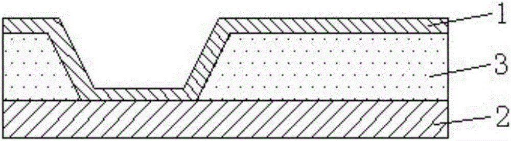
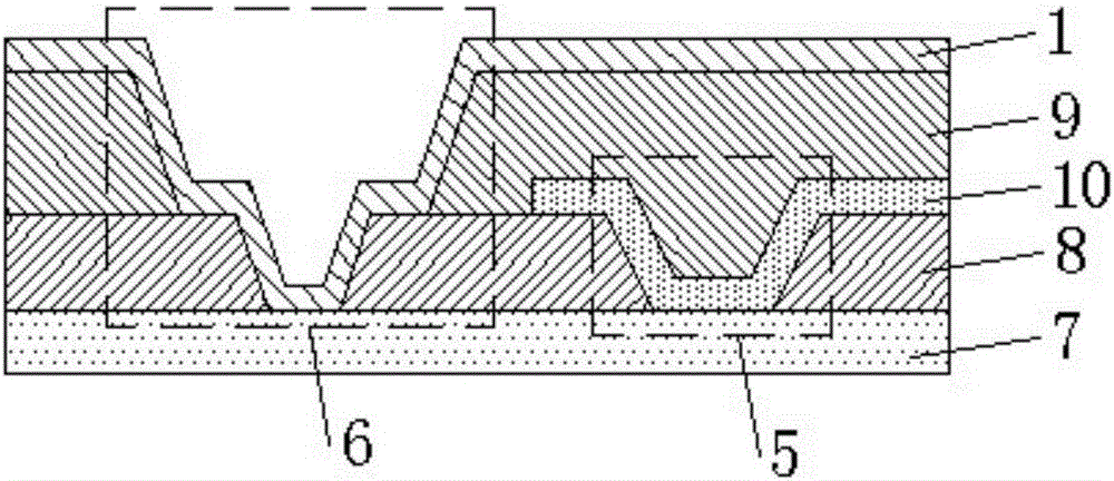
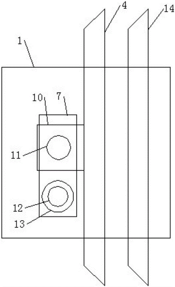
[0038] This embodiment provides an array substrate, figure 2 is a partial cross-sectional view of the array substrate of this embodiment, image 3 It is a perspective view of the partial structure of the array substrate of this embodiment, such as figure 2 , image 3 As shown, the array substrate includes a thin film transistor, a common electrode layer 1 located above the thin film transistor, a touch line 4, and a touch connection terminal 7. The touch connection terminal 7 is arranged in a different layer from the touch line 4 without overlapping. The touch line 4 is connected to the common electrode layer 1 through connection electrodes, wherein the connection electrodes include a first connection electrode 5 and a second connection electrode 6, the touch line 4 is connected to the touch connection terminal 7 through the first connection electrode 5, and the common The electrode layer 1 is connected to the touch connection terminal 7 through the second connection elect...

Embodiment 2

[0046] This embodiment provides a method for preparing an array substrate, which is used to form the array substrate in Embodiment 1. Figure 4 It is a flow chart of the method for preparing the array substrate of this embodiment, as Figure 4 As shown, the method includes the following steps:

[0047] Step S1: forming a figure including a touch connection terminal.

[0048] In this step, it also includes using the same patterning process to form the pattern including the gate on the same layer, that is to say, the pattern of the gate of the thin film transistor and the pattern of the touch connection terminal 7 are formed on the same layer using the same patterning process. In some manufacturing processes of the array substrate, although the touch connection terminal 7 is added in this step, the number of times of the patterning process is not increased. The shape of the touch connection end 7 can be rectangle, circle, ellipse, etc., as long as the touch connection end 7 ha...

Embodiment 3

[0061] This embodiment provides a touch screen, which includes the array substrate in Embodiment 1.

[0062] The touch screen can be specifically a FIC capacitive touch screen, and it can be used in any product or component with display and touch functions, such as liquid crystal display panels, mobile phones, tablet computers, digital cameras, navigators, etc., not only can avoid bad touch and display It appears, and compared with the existing touch screen, it does not increase the number of patterning processes, nor does it increase the manufacturing cost.


PUM


Abstract

The present invention provides an array substrate, a preparation method thereof, and a touch screen, belongs to the display technology field, and can at least partially solve the problem that resistance between a common electrode layer and a touch control line in an existing array substrate is too big, and display and touch control are poor. The array substrate comprises a thin film transistor, and a common electrode layer and a touch control line which are positioned over the thin film transistor; the touch control line and the common electrode layer are connected through connecting electrodes; the connecting electrodes comprise a first connecting electrode and a second connecting electrode; the touch control line is connected with a touch control connecting terminal through the first connecting electrode; and the common electrode layer is connected with the touch control connecting terminal through the second connecting electrode. According to the array substrate, the common electrode layer and the touch control line are indirectly connected through the touch control connecting terminal, resistance between the common electrode layer and the touch control line can be reduced, and poor display and touch control can be prevented.

Description

technical field [0001] The invention belongs to the field of display technology, and in particular relates to an array substrate, a preparation method thereof, and a touch screen. Background technique [0002] A touch screen is also called a touch panel, which has been widely used in various electronic products and widely accepted by consumers. Therefore, the industry has been devoting itself to improving touch screen display technology to bring better user experience to consumers. [0003] Among the existing embedded capacitive touch screens, the touch screens can be divided into On-Cell touch screens and In-Cell touch screens. HIC) capacitive touch screen and fully embedded (Full In-Cell, referred to as FIC) capacitive touch screen. [0004] In the existing FIC capacitive touch screen, the structure of connecting the common electrode layer and the touch line in the array substrate is as follows: figure 1 As shown, an insulating layer 3 is provided between the common elec...

Claims


Application Information

Patent Timeline
IPC IPC(8): G06F3/041
CPCG06F3/041G06F2203/04103G06F3/0445G02F2201/123G06F3/047H01L27/1259
Inventor 史大为
Owner BOE TECH GRP CO LTD
Why Eureka
Try Eureka