
Three-dimensional dbc ceramic circuit board manufacturing method and prepared three-dimensional dbc ceramic circuit board

A manufacturing method and circuit board technology, which can be used in chemical/electrolytic methods to remove conductive materials, printed circuit components, etc., can solve the problems of copper plate etching, poor depth control, poor fluidity of photosensitive dry film, etc. High controllability and smooth hole sides

Active Publication Date: 2018-12-25
NANJING ZHONGJIANG NEW MATERIAL TECH
View PDF2 Cites 0 Cited by
  • Summary
  • Abstract
  • Description
  • Claims
  • Application Information

AI Technical Summary

Problems solved by technology

Photosensitive dry film is an excellent photosensitive material for circuit boards. The circuit boards made of photosensitive dry film have extremely high precision. However, due to the poor fluidity of photosensitive dry film, it can only be used to make circuit boards with a single plane and simple circuits.
Complex circuit boards often have multiple reference planes. At present, photosensitive adhesive can only be used as photosensitive material, because the fluidity and filling property of photosensitive adhesive are far superior to photosensitive dry film.
However, the precision of complex circuit boards made of photosensitive adhesive as photosensitive material, especially DBC (copper-clad ceramic substrate) copper-clad three-dimensional circuit boards, is difficult to guarantee, and when photosensitive adhesive is used as photosensitive material, the sides of the etched holes are often concave inward. The arc-shaped side is formed, and its depth control is relatively poor. It is often easy to corrode the copper plate and fail to meet the line requirements.

Method used


Image

  • Three-dimensional dbc ceramic circuit board manufacturing method and prepared three-dimensional dbc ceramic circuit board
  • Three-dimensional dbc ceramic circuit board manufacturing method and prepared three-dimensional dbc ceramic circuit board
  • Three-dimensional dbc ceramic circuit board manufacturing method and prepared three-dimensional dbc ceramic circuit board

Examples


Embodiment 1

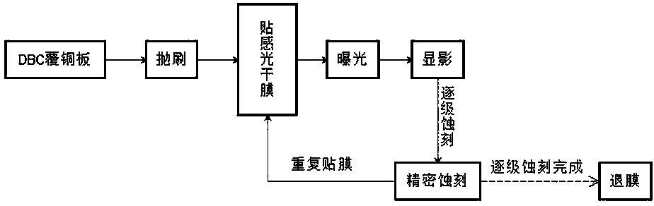
[0041] A method for manufacturing a three-dimensional DBC ceramic circuit board with double reference planes, the steps comprising:

[0042] a. Polish and micro-etch the surface of the DBC copper-clad laminate covered with 0.3mm thick copper to roughen the surface so that it has enough contact area with the photosensitive dry film to increase the bonding force;

[0043] b. Paste photosensitive dry film on the surface of DBC copper clad board in the yellow light room. The film temperature is 115°C, the film pressure is 0.46MP, and the film speed is 0.9m / min. Let it stand for 15 minutes to prevent the photosensitive dry film from thermal expansion and contraction, which will change the size of the exposed pattern. ;

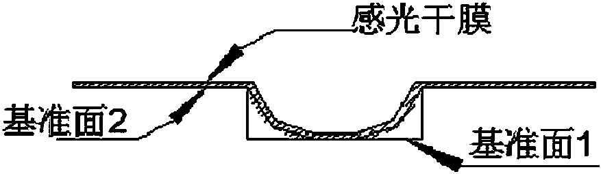
[0044] c. Will be as Figure 6 The shown film 1 with holes is correctly placed on the surface of the DBC copper-clad board pasted with the photosensitive film and covered with the exposure worktable cover to vacuumize, the vacuum degree is -0.06MP, and the exposur...

Embodiment 2

[0049] The three-dimensional DBC ceramic circuit board manufacturing method of three reference planes, the steps include:

[0050] a. Polish and micro-etch the surface of the DBC copper-clad laminate covered with 0.3mm thick copper to roughen the surface so that it has enough contact area with the photosensitive dry film to increase the bonding force;

[0051] b. Paste photosensitive dry film on the surface of DBC copper-clad board in the yellow light room. The film temperature is 115°C, the film pressure is 0.46MP, and the film speed is 0.8m / min. Let stand for 30 minutes to prevent the photosensitive dry film from thermal expansion and contraction, which will change the size of the exposed pattern. ;

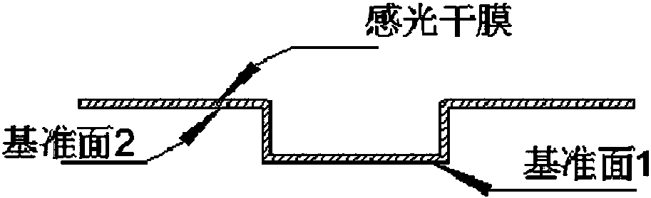
[0052] c. will be as Figure 9 The shown film 1 with holes is correctly placed on the surface of the DBC copper-clad board pasted with the photosensitive film, and the cover plate of the exposure table is vacuumed, the vacuum degree is -0.07MP, and the exposure energy is 23 gr...

Embodiment 3

[0059] A three-dimensional DBC ceramic circuit board manufacturing method with four reference planes, the steps comprising:

[0060] a. Polish and micro-etch the surface of the DBC copper-clad laminate covered with 0.3mm thick copper to roughen the surface so that it has enough contact area with the photosensitive dry film to increase the bonding force;

[0061] b. Paste photosensitive dry film on the surface of DBC copper clad board in the yellow light room. The film temperature is 115°C, the film pressure is 0.46MP, and the film speed is 1.1m / min. Let stand for 25 minutes to prevent the photosensitive dry film from thermal expansion and contraction, which will change the size of the exposed pattern. ;

[0062] c. will be as Figure 9 The shown film 1 with holes is correctly placed on the surface of the DBC copper-clad board pasted with the photosensitive film and covered with the exposure table cover to vacuumize, the vacuum degree is -0.09MP, and the exposure energy is 24 ...


PUM


Abstract

The invention discloses a three-dimensional DBC ceramic circuit board manufacturing method which comprises the steps of firstly performing exposure and developing on the surface of a DBC copper clad laminate by means of a negative film on which holes or combination of holes and a circuit diagram are designed; etching holes with preset depths; then adhering a light-sensitive dry film; then performing exposure, developing and etching on the surface of the DBC copper clad laminate by means of the negative film without holes; and then repeating the steps according to a requirement, thereby obtaining the three-dimensional DBC ceramic circuit board with n reference surfaces on the surface. The three-dimensional DBC ceramic circuit board manufacturing method overcomes a defect that the traditional light-sensitive dry film only can be used for manufacturing a single planar circuit board; through combined application of the film with holes and the light-sensitive dry film, a plurality of different reference films can be accurately etched on the DHC ceramic substrate; and furthermore lines can be etched on each reference surface; high smoothness of the side surface of each etched hole is realized; and high depth controllability is realized.

Description

technical field [0001] The invention relates to a method for manufacturing a three-dimensional DBC ceramic circuit board and the prepared three-dimensional DBC ceramic circuit board, belonging to the technical field of ceramic circuit boards. Background technique [0002] Since the mid-to-late 1980s, electronic products have been developing in the direction of portability, miniaturization, networking, and multimedia. This market demand has put forward corresponding requirements for circuit assembly technology, and the improvement of unit volume information (high density) and The improvement of processing speed per unit time (high speed) has become an important factor to promote the development of microelectronic packaging technology. In order to realize the development of high-density and high-speed circuit modules, the circuit boards are required to develop towards multi-layer, three-dimensional, high temperature resistance, high conductivity, fast heat dissipation, and cor...

Claims


Application Information

Patent Timeline
Patent Type & Authority Patents(China)
IPC IPC(8): H05K3/06H05K1/02
Inventor 尚海瑞井敏黄礼侃赵耀丽
Owner NANJING ZHONGJIANG NEW MATERIAL TECH
Learn More