Packaging structure comprising interconnected embedded chips and flip chips and manufacturing method of packaging structure

A flip-chip, packaging structure technology, applied in semiconductor/solid-state device manufacturing, electrical components, electrical solid-state devices, etc., can solve the problems of incomplete utilization of packaging space, limited number of chip packages, and increased number of chip packages

Inactive Publication Date: 2016-11-16
HUATIAN TECH KUNSHAN ELECTRONICS
View PDF4 Cites 5 Cited by
  • Summary
  • Abstract
  • Description
  • Claims
  • Application Information

AI Technical Summary

Problems solved by technology

[0003] Chinese patent 200410015872.4, a multi-chip integrated circuit packaging method and its structure, discloses a multi-chip packaging process. The chip packaging structure mentioned in the process can effectively increase the number of chip packages and has good heat dissipation performance, but Its packaging space has not been fully utilized, and due to the limitation of the packaging structure, the number of packages of its chips is limited

Method used


Image

  • Packaging structure comprising interconnected embedded chips and flip chips and manufacturing method of packaging structure
  • Packaging structure comprising interconnected embedded chips and flip chips and manufacturing method of packaging structure
  • Packaging structure comprising interconnected embedded chips and flip chips and manufacturing method of packaging structure

Examples


Embodiment 1

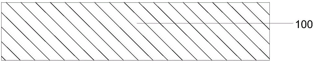
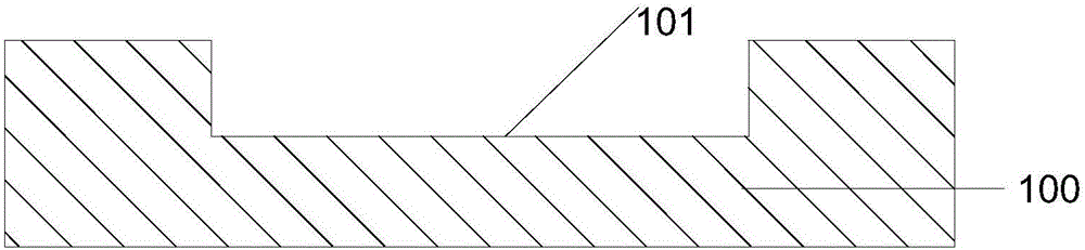
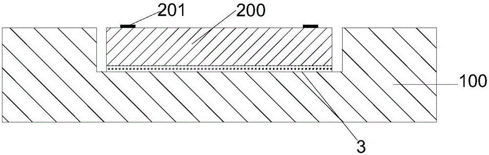
[0047] Such as Figures 1 to 10 As shown, it is the process flow of the manufacturing method of the packaging structure including embedded chips and flip-chip interconnections of the present invention. Such as Figure 10 As shown, a schematic diagram of a packaging structure including embedded chips and flip-chip interconnection in the present invention, the packaging structure includes a silicon substrate 100, and at least one groove 101 is formed on the silicon substrate 100, at least one chip and one The function side of 200 is buried in the groove 101 facing upward. The embedded chip 1 200 forms a plane close to the surface of the silicon substrate 100, and an insulating layer 103 is formed on the plane, and at least one rewiring layer 204 is formed on the insulating layer 103, and at least one chip 2 300 is flip-chip interconnected. On the plane, a first conductive structure 206 is also formed on the plane. The advantage of this is that the packaging volume is small, t...

Embodiment 2

[0063] Such as Figure 11 The structure diagram of another embodiment of the present invention is different from Embodiment 1 in that the flip-chip that is electrically interconnected with the embedded chip and the silicon substrate is two chips: chip three 400 and chip four 500 .

[0064] Preferably, the functions of the chips to be bonded may be the same or different, or not completely the same.

Embodiment 3

[0066] Such as Figure 12 The structure schematic diagram of an embodiment of the present invention is different from the above embodiment in that the groove embedded in the chip is not rectangular.


PUM


Abstract

The invention discloses a packaging structure comprising interconnected embedded chips and flip chips and a manufacturing method of the packaging structure. The packaging structure comprises a substrate and at least one chip I, wherein at least one groove is formed in the substrate; a functional surface of each chip I is upwards embedded into the corresponding groove; the embedded chip I and the surface on which the substrate is located form an approximate plane; an insulating layer is formed on the plane; at least one rewiring layer is formed on the insulating layer; at least one chip II is interconnected to the plane in an inverted manner; and a first conductive structure is also formed on the plane. The at least one chip is embedded into the substrate, and at least one flip chip is electrically interconnected to the embedded chip and the plane in which the substrate is located, so that a plurality of chips can be electrically interconnected, the chip packaging volume is reduced, the process is simple, the packaging structure can be achieved by employing a mature manufacturing technology, and meanwhile, a product is high in yield and good in reliability. The invention further discloses a manufacturing method of the packaging structure.

Description

technical field [0001] The invention relates to a packaging structure in the field of semiconductor chip packaging, in particular to a packaging structure including embedded chips and flip-chip interconnections and a manufacturing method thereof. Background technique [0002] Chip packaging technology is a process technology that wraps the chip to avoid contact between the chip and the outside world and prevent damage to the chip from the outside world. Impurities and bad gases in the air, and even water vapor will corrode the precision circuits on the chip, resulting in a decrease in electrical performance. Different packaging technologies differ greatly in terms of manufacturing processes and processes, and packaging also plays a vital role in the performance of the memory chip itself. With the rapid development of optoelectronic and microelectronic manufacturing technology, electronic products are always developing in the direction of smaller, lighter and cheaper, so the...

Claims


Application Information

Patent Timeline
Patent Type & Authority Applications(China)
IPC IPC(8): H01L23/13H01L23/528H01L21/768H01L21/60
CPCH01L2224/04105H01L2224/12105H01L2224/16227H01L2224/19H01L2224/32225H01L2224/73267H01L2224/92244H01L2924/15153H01L23/13H01L21/76895H01L23/528H01L24/83H01L2224/83365
Inventor 邹益朝于大全
Owner HUATIAN TECH KUNSHAN ELECTRONICS
Why Eureka
Try Eureka