Optical beam combining device of semiconductor laser and optical path control method thereof
A laser and semiconductor technology, applied in optics, optical components, instruments, etc., can solve the problem of low power of a single tube, improve the light output power, and meet the effect of long-distance supplementary light
- Summary
- Abstract
- Description
- Claims
- Application Information
AI Technical Summary
Problems solved by technology
Method used
Image

Examples
Embodiment Construction
[0030] In order to make the object, technical solution and advantages of the present invention more clear and definite, the present invention will be further described in detail below with reference to the accompanying drawings and examples. It should be understood that the specific embodiments described here are only used to explain the present invention, not to limit the present invention.
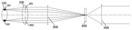
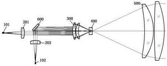
[0031] See figure 1 , figure 1 It is a schematic diagram of the optical path principle of the first preferred embodiment of the semiconductor laser optical beam combining device of the present invention. Such as figure 1 As shown, the semiconductor laser optical beam combining device according to the embodiment of the present invention includes an infrared semiconductor laser 100 , a collimating lens 200 , a focusing lens 300 , a frosted glass 400 and an illumination lens 500 at the rear end arranged in sequence. Among them, the collimating lens is used to convert the light emitted by...
PUM
 Abstract
Description
Claims
Application Information
 - R&D Engineer
- R&D Manager
- IP Professional
- Industry Leading Data Capabilities
- Powerful AI technology
- Patent DNA Extraction
Browse by: Latest US Patents, China's latest patents, Technical Efficacy Thesaurus, Application Domain, Technology Topic.
© 2024 PatSnap. All rights reserved.Legal|Privacy policy|Modern Slavery Act Transparency Statement|Sitemap