A flip-chip deep ultraviolet LED with a double-layer photonic crystal structure and its preparation method

A photonic crystal, deep ultraviolet technology, used in semiconductor devices, nanotechnology for materials and surface science, electrical components, etc., to achieve the effect of improving light output power

Active Publication Date: 2022-02-22
SUZHOU UVCANTEK CO LTD
View PDF9 Cites 0 Cited by
  • Summary
  • Abstract
  • Description
  • Claims
  • Application Information

AI Technical Summary

Problems solved by technology

[0004] The purpose of the present invention is to provide a flip-chip deep ultraviolet LED with a double-layer photonic crystal structure and its preparation method, which is used to solve the problem of strong absorption of deep ultraviolet light by the P-type GaN contact layer and the impact of the sapphire / air interface in the prior art. Total reflection of deep ultraviolet light

Method used


Image

  • A flip-chip deep ultraviolet LED with a double-layer photonic crystal structure and its preparation method
  • A flip-chip deep ultraviolet LED with a double-layer photonic crystal structure and its preparation method
  • A flip-chip deep ultraviolet LED with a double-layer photonic crystal structure and its preparation method

Examples


Embodiment Construction

[0023] The following will clearly and completely describe the technical solutions in the embodiments of the present invention with reference to the accompanying drawings in the embodiments of the present invention. Obviously, the described embodiments are only some, not all, embodiments of the present invention. Based on the embodiments of the present invention, all other embodiments obtained by persons of ordinary skill in the art without making creative efforts belong to the protection scope of the present invention.

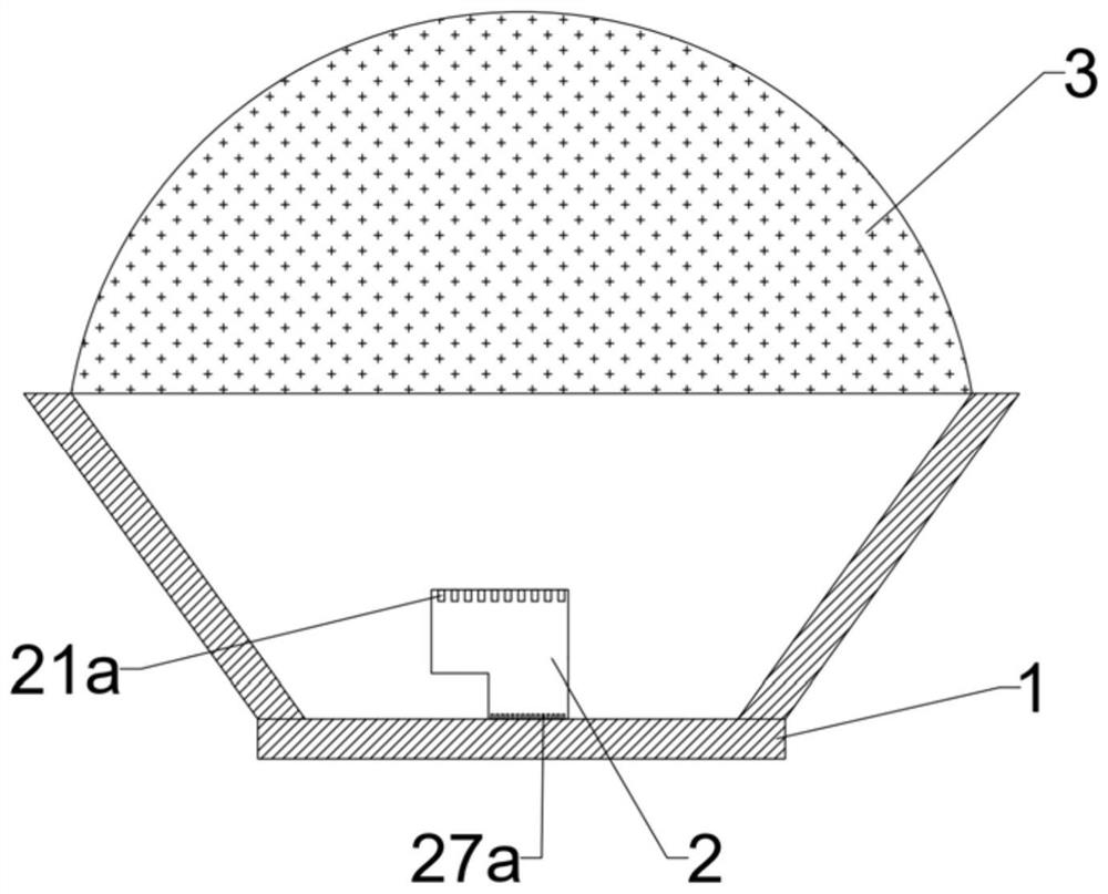
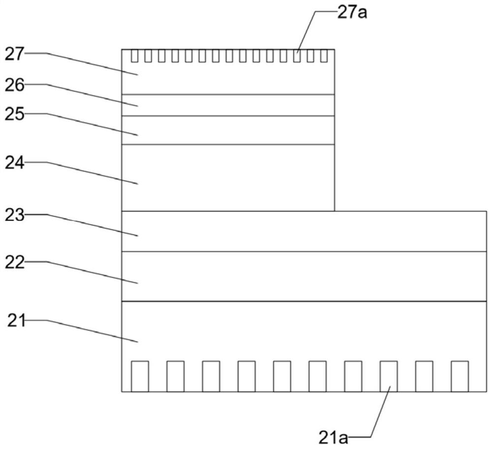
[0024] For the first solution provided by the present invention, please refer to Figure 1~3 , figure 1 It is a structural schematic diagram of an embodiment of a flip-chip deep ultraviolet LED with a double-layer photonic crystal structure in the present invention, figure 2 It is a structural schematic diagram of a deep ultraviolet LED chip in an embodiment of a flip-chip deep ultraviolet LED with a double-layer photonic crystal structure in the present inv...


PUM

PropertyMeasurementUnit
diameteraaaaaaaaaa
depthaaaaaaaaaa
diameteraaaaaaaaaa

Abstract

The invention discloses a flip-chip deep-ultraviolet LED with a double-layer photonic crystal structure and a preparation method thereof. The flip-chip deep-ultraviolet LED with a double-layer photonic crystal structure includes a bracket, a deep-ultraviolet LED chip and a lens, wherein: the lens is set On the top of the support, and the deep ultraviolet LED chip is located in the enclosed space surrounded by the support and the lens; the deep ultraviolet LED chip is arranged at the bottom of the support, and the deep ultraviolet LED chip is close to the support A first nano-array structure is provided on one side surface of the bottom, and a second nano-array structure is provided on a side surface of the deep ultraviolet LED chip away from the bottom of the bracket. The present invention sets the first nano-array structure on the P-type GaN contact layer of the deep-ultraviolet LED, and at the same time sets the second nano-array structure on the sapphire substrate, breaking the existing upper limit of light extraction efficiency and making the light output of the deep-ultraviolet LED The power has more than doubled.

Description

technical field [0001] The invention relates to the field of ultraviolet LED preparation, in particular to a flip-chip deep ultraviolet LED with a double-layer photonic crystal structure and a preparation method thereof. Background technique [0002] Deep ultraviolet LEDs have been widely used in disinfection, sterilization, air purification, food preservation and other fields. However, in terms of the performance of deep ultraviolet LEDs, due to the lower light efficiency (usually less than 5% and changes with the wavelength), especially the limitation of light extraction efficiency, on the one hand, there is still a large distance from the performance of mature commercial blue LEDs. On the other hand, LEDs generate a lot of heat during use and thus affect their life and stability. For the currently relatively mature 280nm deep ultraviolet LED, the light extraction efficiency is still below 10%, and its light loss mainly comes from the total reflection inside the chip and ...

Claims


Application Information

Patent Timeline
Patent Type & Authority Patents(China)
IPC IPC(8): H01L33/46H01L33/00H01L33/48B82Y30/00B82Y40/00
CPCH01L33/46H01L33/0075H01L33/48B82Y30/00B82Y40/00H01L2933/0033H01L2933/0083H01L33/58H01L33/32H01L33/007H01L33/20B82Y20/00
Inventor 陈谦王昊戴江南陈长清
Owner SUZHOU UVCANTEK CO LTD
Why Eureka
Try Eureka