Method and system for testing bonding degree at any position of wafer product

A technology of arbitrary position and test method, applied in the direction of semiconductor/solid-state device test/measurement, electrical components, circuits, etc., can solve the problem of inability to evaluate the degree of bonding, and achieve the effect of simple test method, reduced efficiency and wide application range

Active Publication Date: 2016-12-07
WUHAN XINXIN SEMICON MFG CO LTD
View PDF5 Cites 12 Cited by
  • Summary
  • Abstract
  • Description
  • Claims
  • Application Information

AI Technical Summary

Problems solved by technology

Since the blade can only be inserted into the gapped circumference of the edge of the trimmed wafer, this method can only evaluate the bonding degree of the wafer very close to the edge, usually a few μm from the edge, and cannot The degree of bonding is evaluated at the center of the wafer and most other areas near the center

Method used


Image

  • Method and system for testing bonding degree at any position of wafer product
  • Method and system for testing bonding degree at any position of wafer product

Examples


Embodiment Construction

[0038] The principles and features of the present invention are described below in conjunction with the accompanying drawings, and the examples given are only used to explain the present invention, and are not intended to limit the scope of the present invention.

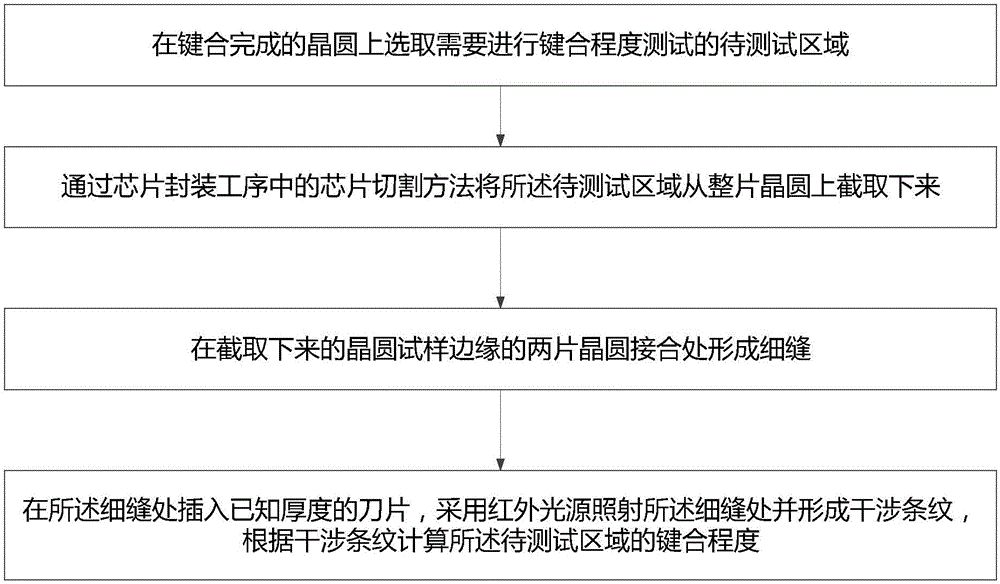
[0039] figure 1 It is a schematic flow chart of a method for testing the degree of bonding at any position on a wafer product in Embodiment 1, including the following steps:

[0040] Step 1. Select the area to be tested on the bonded wafer that needs to be tested for the degree of bonding. The area to be tested can be located at any position on the wafer, such as the edge of the wafer, the center of the wafer, or an area close to the center of the wafer.

[0041] In step 2, the area to be tested is cut off from the entire wafer by a chip cutting method in the chip packaging process. In this embodiment, the region to be tested is cut off from the entire wafer by using a laser method. In other embodiments, a saw blad...


PUM


Abstract

The invention particularly relates to a method and a system for testing the bonding degree at any position of a wafer product. The method comprises the following steps: selecting an area to be tested on a wafer after bonding; cutting out the area to be tested from the whole piece of wafer through a chip cutting method; forming a fine slit at the joint of two pieces of wafers on the edge of the cut wafer sample; inserting a blade at the fine slit, using an infrared source to irradiate at the position of the fine slit and forming interference fringes, and calculating the bonding degree of the area to be tested according to the interference fringes. The method and the system for testing the bonding degree at any position of the wafer provided by the invention can be commonly applied to three-dimensional chip products, the area to be tested of the wafer is cut in virtue of a chip cutting technology, so that the bonding degree at any position of the wafer is tested, and the restriction that the bonding degree at the pole edge position of the wafer can be tested only in a traditional method is overcome; and moreover, the introduction of new working procedures is not needed, so that the efficiency of testing the bonding degree of the wafer cannot be reduced.

Description

technical field [0001] The invention relates to the field of semiconductor manufacturing, in particular to a method and system for testing the bonding degree of any position on a wafer product. Background technique [0002] In the three-dimensional chip (3D-IC) technology, such as the process of preparing BSI, UTS and other products, two wafers need to be bonded, and the degree of bonding of the wafers has a great impact on the entire process and the performance of the final product. Therefore, The degree of bonding needs to be evaluated after the bonding process. The prior art generally adopts the method of inserting a blade to evaluate the bonding degree at the edge of the entire wafer, specifically: a thin blade of known thickness is inserted at the edge (edge) of the wafer processed by trimming, according to The interference fringes formed after the irradiation of the infrared light source are combined with the formula to calculate the surface energy at the insertion bl...

Claims


Application Information

Patent Timeline
Patent Type & Authority Applications(China)
IPC IPC(8): H01L21/66
CPCH01L22/12H01L22/30
Inventor 仝金雨李辉李品欢李桂花肖科
Owner WUHAN XINXIN SEMICON MFG CO LTD
Why Eureka
Try Eureka