Multi-Chip Stack Package Structure
A technology of packaging structure and chip stacking, which is used in semiconductor/solid-state device components, semiconductor devices, electrical components, etc., and can solve problems such as not being able to fully meet requirements
- Summary
- Abstract
- Description
- Claims
- Application Information
AI Technical Summary
Problems solved by technology
Method used
Image

Examples
Embodiment Construction
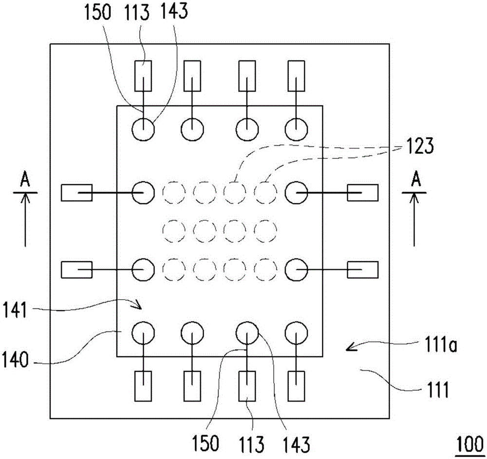
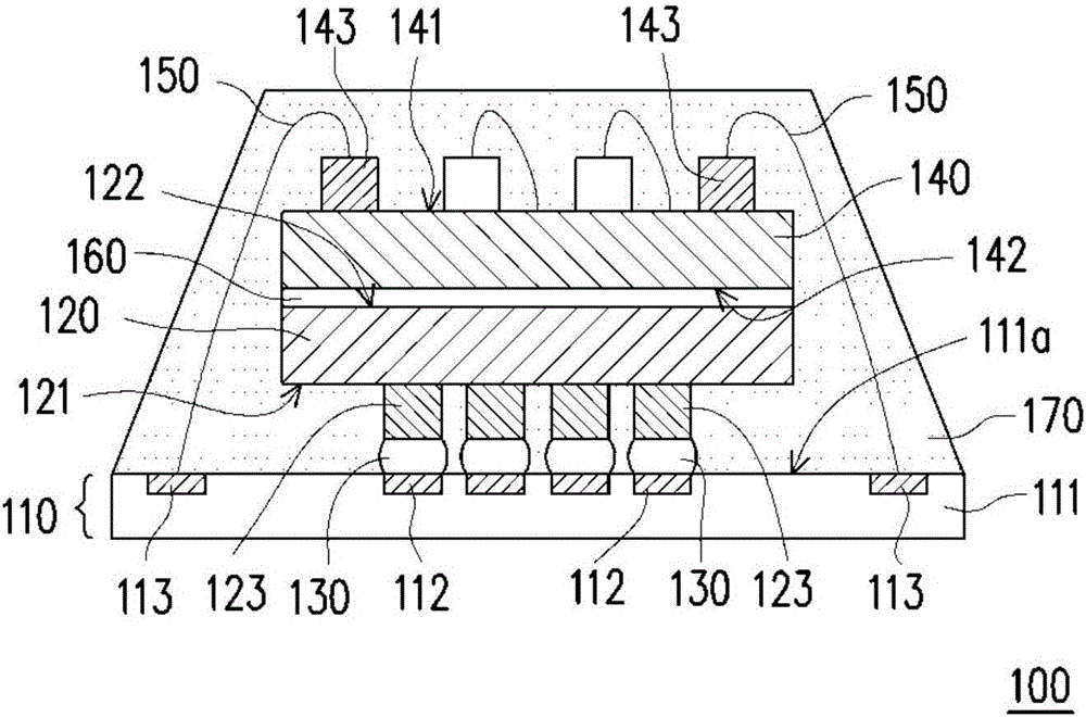
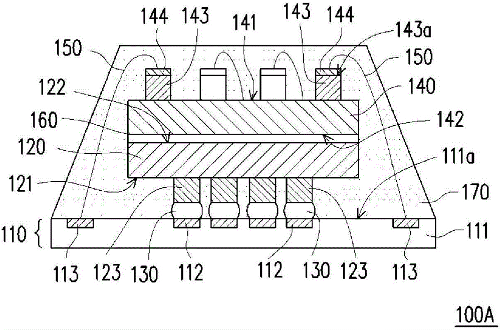
[0041] figure 1 It is a top view of a chip stack package structure according to an embodiment of the present invention. figure 2 yes figure 1 The cross-sectional schematic diagram of the chip stack package structure along the line A-A, for clarity and convenience of description, figure 1 The encapsulant 170 is omitted from illustration. Please refer to figure 1 and figure 2 , in this embodiment, the chip stack package structure 100 includes a circuit carrier 110, a first chip 120, a plurality of solder balls 130, a second chip 140 and a plurality of bonding wires 150, wherein the substrate 111 of the circuit carrier 110 The material is, for example, a material commonly used as a base material of a printed circuit board, such as FR4, FR5 or BT material. However, the material of the base material 111 of the circuit carrier 110 is not limited to the materials such as FR4, FR5 or BT mentioned above, the base material 111 of the circuit carrier 110 can also be made of polyim...
PUM
 Abstract
Description
Claims
Application Information
 - R&D
- Intellectual Property
- Life Sciences
- Materials
- Tech Scout
- Unparalleled Data Quality
- Higher Quality Content
- 60% Fewer Hallucinations
Browse by: Latest US Patents, China's latest patents, Technical Efficacy Thesaurus, Application Domain, Technology Topic, Popular Technical Reports.
© 2025 PatSnap. All rights reserved.Legal|Privacy policy|Modern Slavery Act Transparency Statement|Sitemap|About US| Contact US: help@patsnap.com