
Bottom gap welding method for LCCC apparatus

A technology of gap welding and devices, which is applied in the field of circuits, can solve problems such as failure of LCCC devices and PCB components, cracks in brittle LTCC shells, lack of size, etc., and achieve the effects of improving tangential deformation capacity, alleviating the influence of thermal stress, and improving fatigue life

Inactive Publication Date: 2016-12-14
NORTH ELECTRON RES INST ANHUI CO LTD
View PDF7 Cites 1 Cited by
  • Summary
  • Abstract
  • Description
  • Claims
  • Application Information

AI Technical Summary

Problems solved by technology

There are two obvious defects in this soldering method: one is that it is difficult to effectively remove the flux residue accumulated in the bottom gap of components after soldering through conventional cleaning process; the other is that the size of tin-lead solder in the thickness direction is very small and There is almost no pure solder layer, resulting in poor fatigue life of solder joints against temperature changes
[0003] In addition, for devices packaged in LCCC (leadless ceramic chip carrier) made of LTCC (low temperature co-fired ceramic) materials, the coefficient of thermal expansion (CTE) of the LTCC shell and PCB board are respectively 5.8ppm / °C and 15ppm / °C~ 17ppm / ℃, the mismatch of CTE between the two can easily cause the brittle LTCC shell of the larger LCCC package device to crack or even break due to excessive thermal stress in a temperature shock environment, resulting in failure of LCCC devices and PCB components

Method used


Image

  • Bottom gap welding method for LCCC apparatus
  • Bottom gap welding method for LCCC apparatus
  • Bottom gap welding method for LCCC apparatus

Examples


Embodiment Construction

[0031] The present invention will be further described below in conjunction with the accompanying drawings. The following examples are only used to illustrate the technical solution of the present invention more clearly, but not to limit the protection scope of the present invention.

[0032] The technical scheme of the patent application for the present invention is:

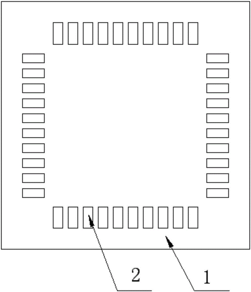
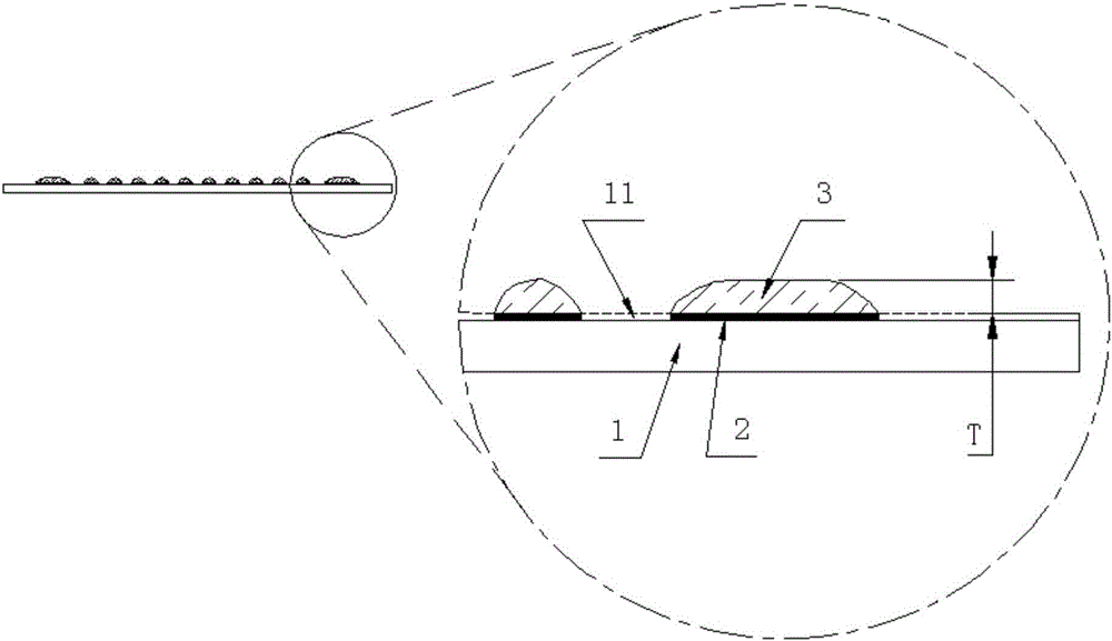
[0033] 1) Pre-soldering: Use a mask with a suitable thickness, and mount the pad 2 of the LCCC device on the PCB board 1 ( Figure 1a , Figure 1b ) printed a layer of tin-lead solder paste on the surface, and after the general reflow soldering and cleaning process, each pad of the PCB board is covered with a layer of thickness (the height above the solder mask layer 11 on the upper surface of the PCB board) is T, thickness Solid tin-lead solder layer with good uniformity 3 ( Figure 2a , Figure 2b );

[0034] 2) Dispensing SMT adhesive: use SMT dispensing machine, set appropriate dispensing parameters, an...


PUM

PropertyMeasurementUnit
Thicknessaaaaaaaaaa
Thicknessaaaaaaaaaa

Abstract

The invention discloses a bottom gap welding method for an LCCC apparatus. The method comprises the following steps: 1) covering the surface of an LCCC apparatus mounting pad of a PCB board with a solid tin-lead solder layer; 2) dispensing a central position where the LCCC apparatus is mounted on the surface of the PCB board with a drop of a surface mount adhesive; 3) aligning the LCCC apparatus to the LCCC apparatus mounting position on the PCB board and pressing the LCCC apparatus till the leading-out end of a bottom surface metalized film layer of the LCCC apparatus falls onto the solid tin-lead solder layer; 4) curing the surface mount adhesive; and 5) dispensing tin-lead solder paste and then performing reflow soldering on the LCCC apparatus and the PCB board. A certain gap is reserved between the bottom surface of the LCCC apparatus and the upper surface of the PCB board, so that soldering flux residues in the tin-lead solder are easily cleaned; the tangential deformation capacity of a welding point is improved due to increase of height of a welding flux connecting point, the thermal stress influence generated by temperature variation can be effectively alleviated, the fatigue life of the welding point is prolonged and the thermal shock resistance of an LCCC packaging housing is improved, and occurrence of failures of the apparatus and assemblies is reduced.

Description

technical field [0001] The invention relates to a bottom gap welding method of an LCCC device, in particular to a process method for leaving a 0.2mm-0.3mm gap at the bottom when welding an LCCC device on a PCB, and belongs to the field of circuit technology. Background technique [0002] The installation of leadless surface-mount electronic components on PCB (printed circuit) boards usually uses SMT (surface mount technology) technology to achieve soldering by tin-lead solder, leaving no gap between the bottom of the component and the surface of the PCB board . There are two obvious defects in this soldering method: one is that it is difficult to effectively remove the flux residue accumulated in the bottom gap of components after soldering through conventional cleaning process; the other is that the size of tin-lead solder in the thickness direction is very small and There is almost no pure solder layer, resulting in poor fatigue life of solder joints against temperature c...

Claims


Application Information

Patent Timeline
IPC IPC(8): B23K1/012B23K1/20
CPCB23K1/206B23K1/012
Inventor 何中伟周冬莲薛峻宋哲宇
Owner NORTH ELECTRON RES INST ANHUI CO LTD
Learn More