Converting circuit and working method thereof, compensation device and display device

A conversion circuit and voltage terminal technology, applied in static indicators, instruments, etc., can solve problems such as affecting compensation effect and conversion accuracy loss, and achieve the effect of achieving brightness, avoiding conversion accuracy loss, and uniform display.

Inactive Publication Date: 2016-12-21
BOE TECH GRP CO LTD
View PDF5 Cites 4 Cited by
  • Summary
  • Abstract
  • Description
  • Claims
  • Application Information

AI Technical Summary

Problems solved by technology

[0004] In order to solve the above problems, the present invention provides a conversion circuit and its working method, a compensation device and a display device, which at least partiall

Method used


Image

  • Converting circuit and working method thereof, compensation device and display device
  • Converting circuit and working method thereof, compensation device and display device
  • Converting circuit and working method thereof, compensation device and display device

Examples


Embodiment 1

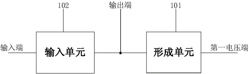
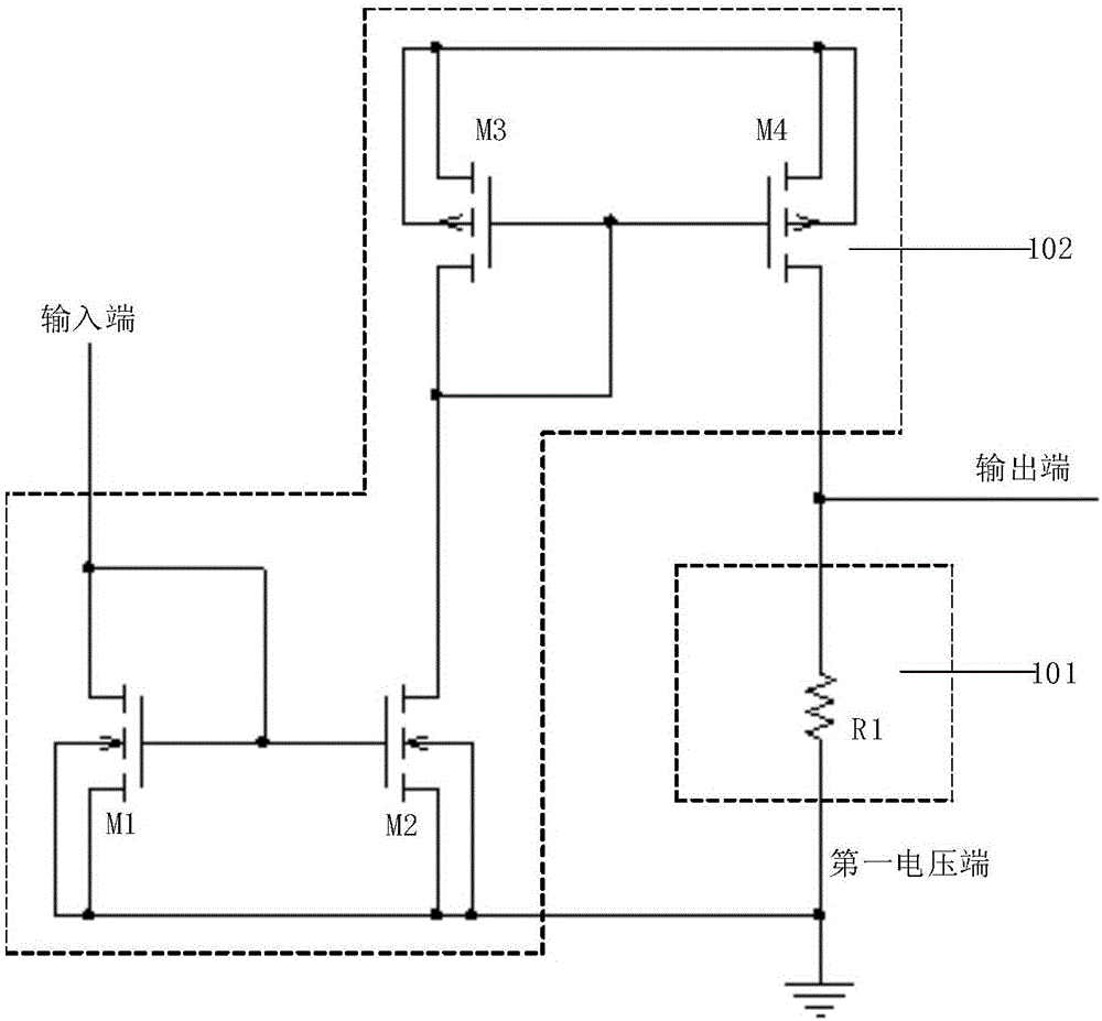
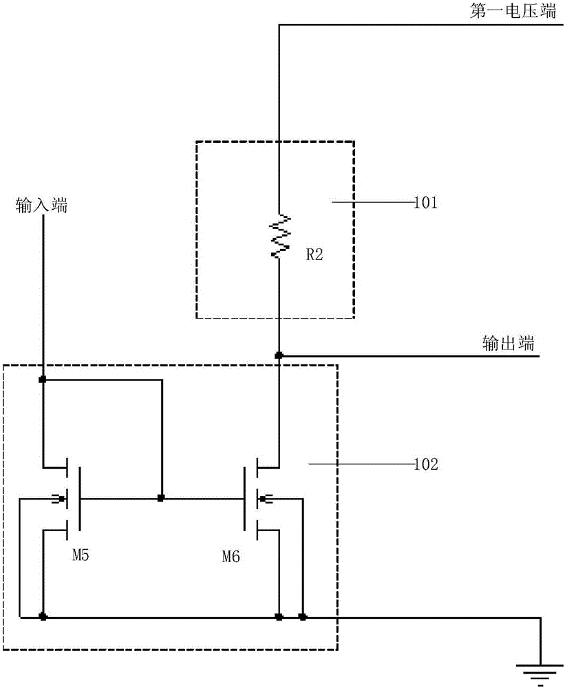
[0039] figure 1 It is a schematic structural diagram of a conversion circuit provided by Embodiment 1 of the present invention. Such as figure 1 As shown, the conversion circuit includes a forming unit 101 and an input unit 102, the forming unit 101 is respectively connected to the output terminal and the first voltage terminal, and the input unit 102 is respectively connected to the input terminal and the output terminal. The forming unit 101 is used to form a standard resistor according to a standard current and a preset voltage, and the input unit 102 is used to output the driving current to the standard resistor according to the driving current input from the input terminal. The forming unit 101 It is used for forming a voltage signal according to the input signal of the first voltage terminal and the driving current. The technical solution provided in this embodiment forms a standard resistance according to the standard current and preset voltage, so that the resistance...

Embodiment 2

[0048] Figure 5 It is a schematic structural diagram of a compensation device provided in Embodiment 2 of the present invention. Such as Figure 5 As shown, the compensation device includes a compensation unit 103 and the conversion circuit provided in Embodiment 1, the conversion circuit includes a forming unit 101 and an input unit 102, and the forming unit 101 is connected to the compensation unit 103 and the first voltage terminal respectively, The input unit 102 is connected to the input terminal and the compensation unit 103 respectively. For the specific content of the conversion circuit, reference may be made to the description of Embodiment 1, which will not be repeated here.

[0049] In the compensation device provided in this embodiment, the conversion circuit includes a forming unit and an input unit, the forming unit is respectively connected to the output terminal and the first voltage terminal, and the input unit is respectively connected to the input termina...

Embodiment 3

[0051] Image 6 It is a schematic structural diagram of a display device provided by Embodiment 3 of the present invention. Such as Image 6 As shown, the display device includes a pixel unit 104 and the compensation device provided in Embodiment 2. The compensation device includes a compensation unit 103, a forming unit 101, and an input unit 102. The forming unit 101 is connected to the compensation unit 103 and the first The voltage terminal is connected, and the input unit 102 is respectively connected with the pixel unit 104 and the compensation unit 103 . For details about the compensation device, reference may be made to the description of Embodiment 2, which will not be repeated here.

[0052] In the display device provided in this embodiment, the conversion circuit includes a forming unit and an input unit, the forming unit is respectively connected to the output terminal and the first voltage terminal, and the input unit is respectively connected to the input termi...


PUM


Abstract

The invention discloses a converting circuit and a working method thereof, a compensation device and a display device. The converting circuit comprises a forming unit and an input unit; the forming unit is connected with an output terminal and a first voltage terminal; and the input unit is connected with an input terminal and the output terminal. The forming unit is used for forming a standard resistor according to a standard current and a preset voltage; the input unit is used for outputting a driving current according to the driving current inputted by the input terminal; and the forming unit is used for forming a voltage signal based on an input signal of the first voltage terminal and the driving current. According to the technical scheme, the standard resistor is formed based on the standard current and the preset voltage and thus the resistor precision is set at a same value, so that a pixel driving current can be converted into a voltage signal accurately and thus the conversion precision loss caused by the individual resistor difference can be avoided.

Description

technical field [0001] The invention relates to the field of display technology, in particular to a conversion circuit and its working method, a compensation device and a display device. Background technique [0002] In an existing pixel circuit, a driving transistor TFT (Thin Film Transistor, TFT) is driven to be turned on by a data voltage to generate a driving current to act on an OLED (Organic Light-Emitting Diode, OLED), thereby driving the OLED to emit light. Due to the uncontrollable factors in the process and actual production, the characteristics of the driving tube TFTs are not completely the same or even vary greatly, so the same data voltage acts on different driving tube TFTs to generate different or even large differences in current, thus This leads to uneven brightness of the OLED. [0003] In order to solve the above problems, the prior art adjusts the driving data so that the driving current of the driving transistor TFT reaches a desired value. During the...

Claims


Application Information

Patent Timeline
IPC IPC(8): G09G3/3233
CPCG09G3/3233G09G2320/0233G09G3/3283G09G2310/0272G09G2310/0289G09G2320/0223
Inventor 宋琛吴仲远
Owner BOE TECH GRP CO LTD
Why Eureka
Try Eureka