Semiconductor structure and method of forming the same

A technology of semiconductors and regular polygons, which is applied in the direction of semiconductor devices, semiconductor/solid-state device manufacturing, semiconductor/solid-state device components, etc., can solve problems such as fracture or falling off, chip package failure, and affecting product yield, so as to achieve the goal of not being easily broken or The effect of shedding and uniform stress distribution

Active Publication Date: 2019-07-05
JIANGSU NEPES SEMICON
View PDF7 Cites 0 Cited by
  • Summary
  • Abstract
  • Description
  • Claims
  • Application Information

AI Technical Summary

Problems solved by technology

[0003] However, at present, the metal bumps formed by the existing technology often have problems such as breakage or falling off when entering the packaging process, resulting in chip packaging failure and affecting product yield.
[0004] Therefore, the performance of the existing metal bumps needs to be further improved

Method used


Image

  • Semiconductor structure and method of forming the same
  • Semiconductor structure and method of forming the same
  • Semiconductor structure and method of forming the same

Examples


Embodiment Construction

[0021] Specific implementations of the semiconductor structure and its forming method provided by the present invention will be described in detail below in conjunction with the accompanying drawings.

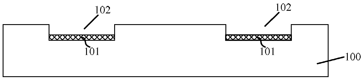
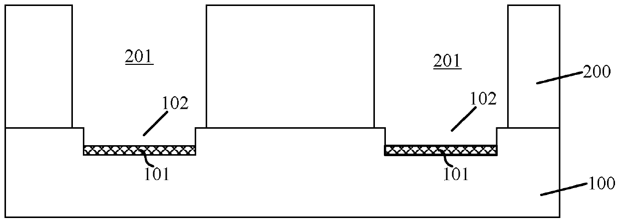
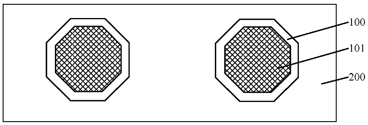
[0022] Please refer to figure 1 , providing a substrate 100, the surface of the substrate 100 has a groove 101, and the groove 102 exposes the surface of the metal layer 101.

[0023] The substrate 100 is a multi-layer structure, including a semiconductor layer and a dielectric layer located on the surface of the semiconductor layer, a semiconductor device located in the semiconductor layer, a metal interconnection structure in the dielectric layer, and the like. The metal layer 101 is a solder pad, which serves as a connection structure with an external circuit after packaging, and the material of the metal layer 101 can be metal such as Al, Cu or Au. The size of the metal layer 101 may be the same as the size of the groove 102 or larger than the size of the groove 102 .

...


PUM


Abstract

The invention discloses a semiconductor structure and a forming method thereof. The semiconductor structure comprises a substrate, wherein the surface of the substrate is provided with a groove. The groove is exposed out of the surface of a metal layer. A metal bump is positioned on the surface of the metal layer and on the partial surface of the substrate. The shape of the cross section of the metal bump is the same as the shape of the cross section of the groove. The vertical distances between the sidewalls of the metal bump and the sidewalls of the groove are the same. The metal bump in the semiconductor structure is not easy to break or fall off.

Description

technical field [0001] The invention relates to the technical field of semiconductors, in particular to a semiconductor structure and a forming method thereof. Background technique [0002] With the continuous development of semiconductor technology, the integration level of integrated circuits is getting higher and higher, and metal bump technology, as an important technology of flip-chip welding process, has been more and more widely used. The metal bump technology is usually applied in the flip-chip packaging technology. Metal bumps are formed on the surface of the connecting metal layer of the chip, and then the chip is connected to the substrate through the metal bumps through reflow. [0003] However, at present, the metal bumps formed by the prior art often have problems such as breakage or falling off when entering the packaging process, which leads to the failure of chip packaging and affects the yield of products. [0004] Therefore, the performance of the existin...

Claims


Application Information

Patent Timeline
Patent Type & Authority Patents(China)
IPC IPC(8): H01L21/60H01L23/488
CPCH01L24/10H01L24/11H01L24/12H01L2224/11
Inventor 杨雪松谢志峰
Owner JIANGSU NEPES SEMICON
Why Eureka
Try Eureka