Chemical vapor deposition apparatus and deposition method thereof

A chemical vapor deposition and exhaust device technology, which is applied in the direction of gaseous chemical plating, metal material coating process, coating, etc., to achieve the effect of reducing deposition, increasing distance, and reducing manufacturing difficulty

Active Publication Date: 2019-02-15
ADVANCED MICRO FAB EQUIP INC CHINA
View PDF7 Cites 0 Cited by
  • Summary
  • Abstract
  • Description
  • Claims
  • Application Information

AI Technical Summary

Problems solved by technology

[0008] Therefore, in the prior art, improving productivity and improving product yield constitute a pair of contradictions that are difficult to overcome

Method used


Image

  • Chemical vapor deposition apparatus and deposition method thereof
  • Chemical vapor deposition apparatus and deposition method thereof
  • Chemical vapor deposition apparatus and deposition method thereof

Examples


Embodiment Construction

[0065] The present invention will be described in detail below in conjunction with the accompanying drawings.

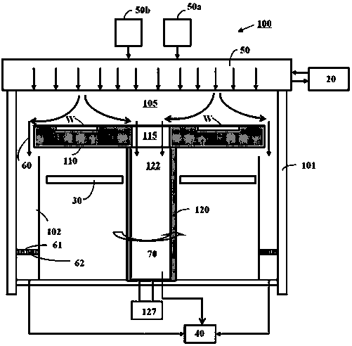
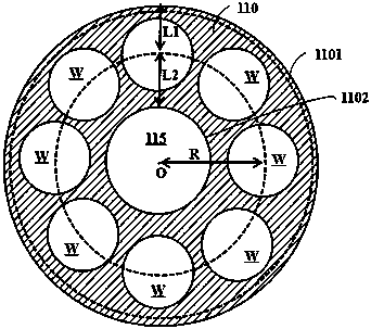
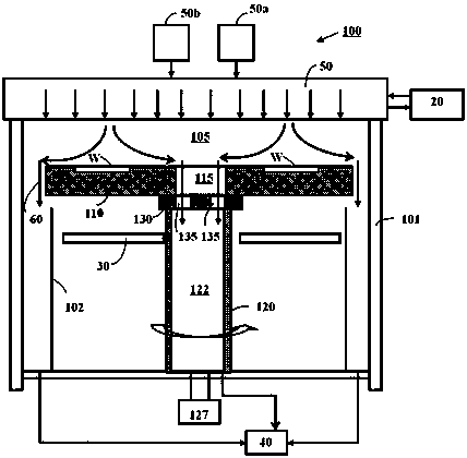
[0066] The invention provides a chemical vapor deposition reaction device and a deposition method for depositing thin films or growing epitaxial crystals on substrates or substrates. The reaction device and the deposition method can be used to deposit various thin films on the substrate or on the substrate. In particular, the reaction device of the present invention can be preferably applied to the MOCVD method or the HVPE method to deposit or epitaxially grow III-V group thin films.

[0067] The chemical vapor deposition device provided by the present invention can realize the simultaneous processing of multiple substrates in one reaction chamber, and ensure the yield and uniformity of each substrate as in a single substrate reaction chamber, thereby not only improving The yield and uniformity of deposited or epitaxially grown films can greatly increase the yield, a...


PUM


Abstract

The invention discloses a chemical vapor deposition device which comprises a reaction chamber and a gas inlet device. A substrate tray and a rotary shaft are arranged in the reaction chamber, the substrate tray is used for supporting a plurality of substrates, the gas inlet device is arranged above a substrate bearing device and used for providing reaction gas flowing to the surfaces of the substrates, and a reaction area is formed between the gas inlet device and the substrate bearing device. A central exhaust system is arranged in the center area of the substrate bearing device. An annular edge exhaust system is arranged around the substrate bearing device. The reaction gas and side reaction gas on the surface of each substrate are exhausted out of the reaction chamber through the central exhaust system and the edge exhaust system at the same time. The thin film deposition yield and uniformity of the surfaces of the substrates can be effectively adjusted.

Description

technical field [0001] The invention relates to a device for depositing a thin film on a substrate, in particular to a reaction chamber and a deposition method for depositing or epitaxially growing a thin film with high yield and uniformity on the substrate. Background technique [0002] As one of the III-V thin films, gallium nitride (GaN) is a material widely used in the manufacture of blue, violet and white light diodes, ultraviolet detectors and high-power microwave transistors. Growth of GaN thin films has received great attention due to GaN's actual and potential use in fabricating low-energy devices (eg, LEDs) for a wide range of applications. [0003] III-V films, including GaN films, can be grown in a number of different ways, including molecular beam epitaxy (MBE), hydride vapor phase epitaxy (HVPE), metal organic compound chemical vapor deposition (MOCVD), etc. . Currently, the MOCVD method is the preferred deposition method for obtaining thin films of sufficien...

Claims


Application Information

Patent Timeline
Patent Type & Authority Patents(China)
IPC IPC(8): C23C16/44C23C16/455
Inventor 幸沛锦杜志游
Owner ADVANCED MICRO FAB EQUIP INC CHINA
Why Eureka
Try Eureka