Integrated touch display panel and touch display device thereof

一种触控显示面板、集成的技术,应用在仪器、半导体器件、计算等方向,能够解决影响触控精度、信号干扰、信噪比降低等问题,达到提高信噪比和触控精度、避免触控不良的效果

Active Publication Date: 2017-01-04
XIAMEN TIANMA MICRO ELECTRONICS +1
View PDF5 Cites 7 Cited by
  • Summary
  • Abstract
  • Description
  • Claims
  • Application Information

AI Technical Summary

Problems solved by technology

[0004] There will be signal interference between adjacent touch drive electrodes, which will reduce the signal-to-noise ratio and affect the touch accuracy

Method used


Image

  • Integrated touch display panel and touch display device thereof
  • Integrated touch display panel and touch display device thereof
  • Integrated touch display panel and touch display device thereof

Examples


Embodiment 1

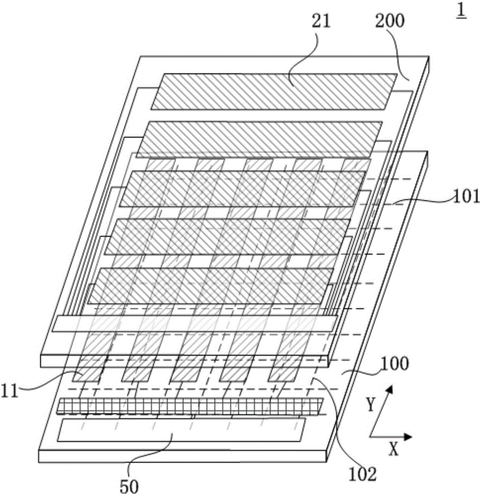
[0034] Such as figure 1 Shown is a schematic structural diagram of the integrated touch display panel of Embodiment 1 of the present invention; the integrated touch display panel 1 of Embodiment 1 includes an array substrate 100 and a color filter substrate 200 arranged oppositely, and the array substrate 100 and the color filter substrate 200 include The display area and the non-display area surrounding the display area.

[0035] figure 1 Although the display area and non-display area are not specifically identified in , optionally, figure 1 The criss-cross electrode area in the middle as shown corresponds to the display area, and the area around the display area is the non-display area. figure 1 The leads and circuit parts shown in are set in the non-display area.

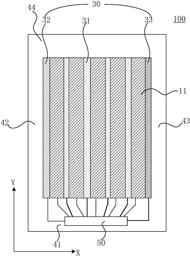
[0036] Such as figure 1 with figure 2 As shown, in the display area, the array substrate 100 is provided with several strips along the first direction ( figure 1 shown in the Y direction) and extend along ...

Embodiment 2

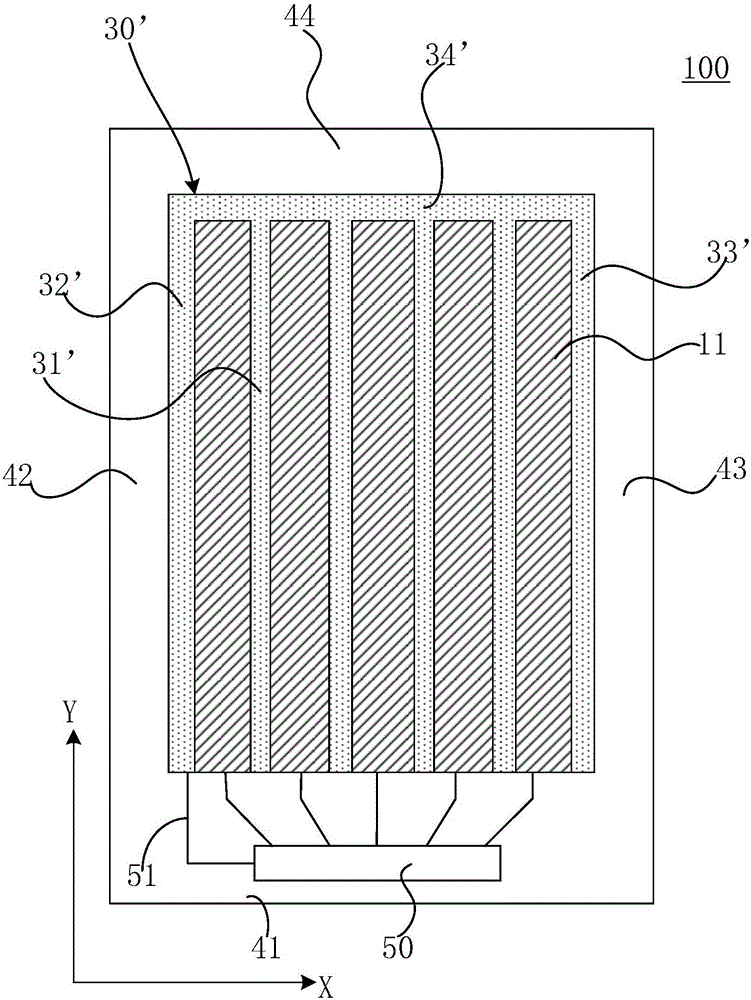
[0051] The difference between the integrated touch display panel of Embodiment 2 and Embodiment 1 lies in the shielding structure 30'.

[0052] Such as image 3 As shown, the shielding structure 30' of Embodiment 2 has several first shielding electrodes 31' disposed between two adjacent touch driving electrodes 11, and touch driving electrodes disposed adjacent to the second non-display area 42. 11 (ie image 3 The second shielding electrode 32' between the leftmost touch driving electrode 11) and the touch driving electrode 11 arranged in the third non-display area 43 adjacent to it (i.e. image 3 The third shielding electrode 33' between the rightmost touch driving electrodes 11) in the middle; the first shielding electrode 31', the second shielding electrode 32' and the third shielding electrode 33' are the same as the corresponding structures in Embodiment 1 , so details will not be repeated here.

[0053] Such as image 3 As shown, the shielding structure 30' of Embod...

Embodiment 3

[0067] The difference between the integrated touch display panel of Embodiment 3 and Embodiment 2 lies in the shielding structure 30 ″.

[0068] Such as Figure 4 As shown, in the shielding structure 30 ″ of Embodiment 3, one or more disconnection points (not marked in the figure) may be provided on the fourth shielding electrode 34 ″.

[0069] Such as Figure 4 As shown, preferably, in this embodiment, the fourth shielding electrode 34" is provided with several disconnection points corresponding to each touch driving electrode 11 in turn, so that the fourth shielding electrode is blocked by these disconnection points Divided into several fourth shielding sub-electrodes 34a".

[0070] Such as Figure 4 As shown, the fourth shielding sub-electrode 34a" is sequentially connected to an adjacent first shielding electrode 31" to form a "┏"-shaped electrode structure.

[0071] Specifically, as Figure 4 As shown, in Embodiment 3, the left end point of each fourth shielding sub-...


PUM


Abstract

The invention relates to an integrated touch display panel and a touch display device thereof. A shielding structure is arranged on an array substrate of the integrated touch display panel disclosed by the invention, and the shielding structure comprises a plurality of first shielding electrodes that extend along a first direction and are arranged along a second direction and between two adjacent touch drive electrodes. Compared with the prior art, the integrated touch display panel disclosed by the invention can better shield signal interference and coupling interference between any two adjacent touch drive electrodes, thus preventing poor touch caused thereby and increasing the signal-to-noise ratio and touch precision.

Description

technical field [0001] The invention relates to an integrated touch display panel and a touch display device thereof. Background technique [0002] With the development of display technology, more and more display panels are integrated with touch functions to bring convenience to users. [0003] At present, in order to reduce the thickness of the display panel and realize the touch function, the touch structure is usually integrated into the display panel. For example, in the existing mutual capacitive hybrid touch structure (hybrid in-cell), the touch driving electrodes (TX electrodes) are arranged on the inner side of the array substrate (TFT substrate), and the touch sensing electrodes (RX electrodes) are arranged on the inner side of the color array substrate. The outer side of the film substrate (CF substrate), in which the common electrode (Vcom) of the display panel is divided into several strip-shaped sub-electrodes extending along the direction of the data lines an...

Claims


Application Information

Patent Timeline
Patent Type & Authority Applications(China)
IPC IPC(8): G06F3/041
CPCG06F3/041G06F3/0418G06F3/0412H01L27/1214G06F2203/04107G06F3/0446G06F3/0445
Inventor 庄知龙黄建才许育民
Owner XIAMEN TIANMA MICRO ELECTRONICS
Why Eureka
Try Eureka