Supercharge Your Innovation With Domain-Expert AI Agents!

A kind of superjunction mosfet structure and preparation method thereof

A silicon substrate, heavy doping technology, applied in semiconductor/solid-state device manufacturing, semiconductor devices, electrical components, etc., can solve the problems of poor stability and complicated preparation process of super-junction MOSFETs, achieve small on-resistance and reduce manufacturing costs. cost, and the effect of improving breakdown resistance characteristics

Active Publication Date: 2019-10-15
FOUNDER MICROELECTRONICS INT
View PDF1 Cites 0 Cited by
  • Summary
  • Abstract
  • Description
  • Claims
  • Application Information

AI Technical Summary

Problems solved by technology

[0007] In order to solve the above technical problems, the present invention provides a super junction MOSFET structure and its preparation method, which solves the problems of poor stability and complicated preparation process of super junction MOSFET

Method used


Image

  • A kind of superjunction mosfet structure and preparation method thereof
  • A kind of superjunction mosfet structure and preparation method thereof
  • A kind of superjunction mosfet structure and preparation method thereof

Examples


Embodiment

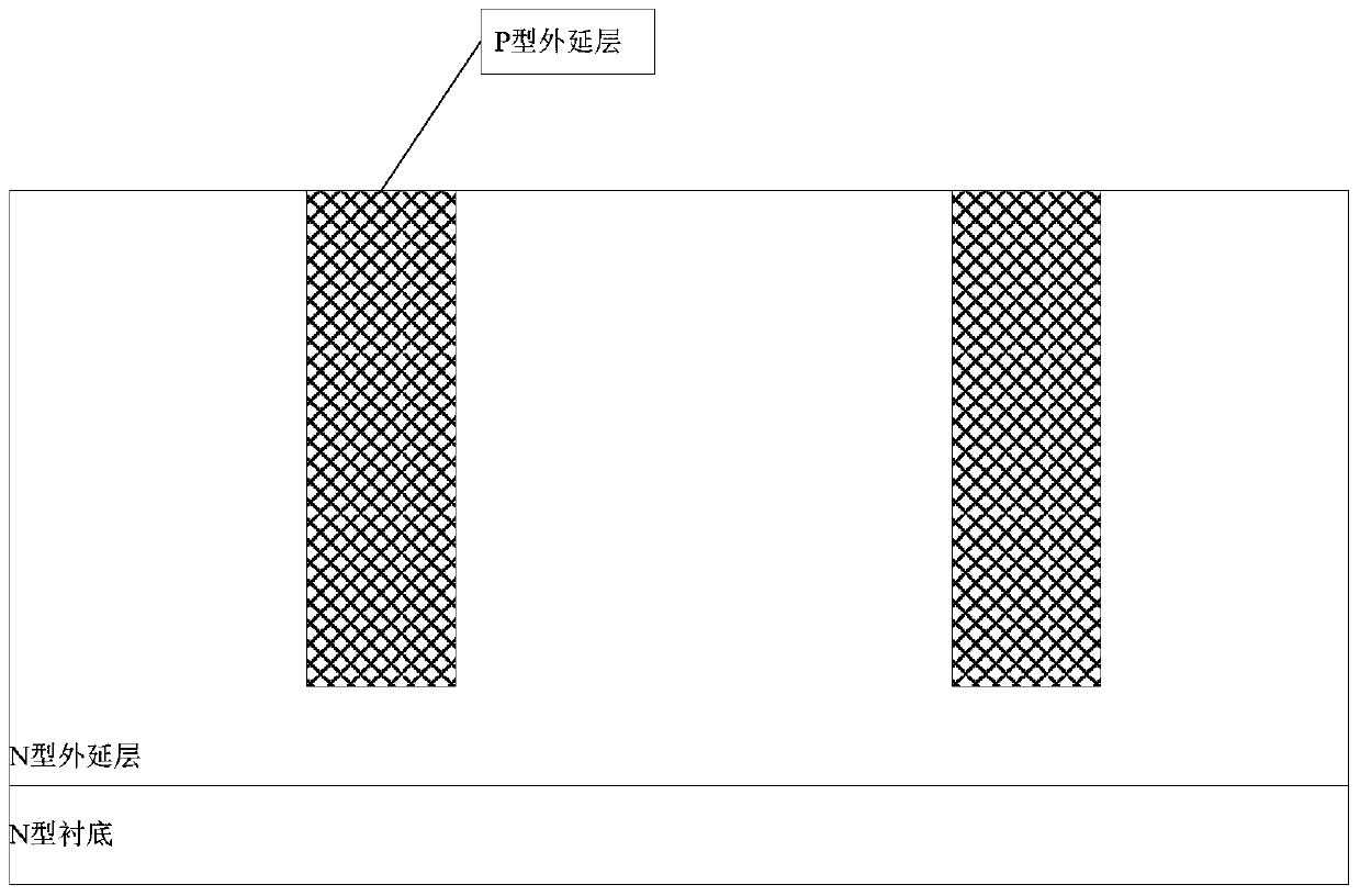
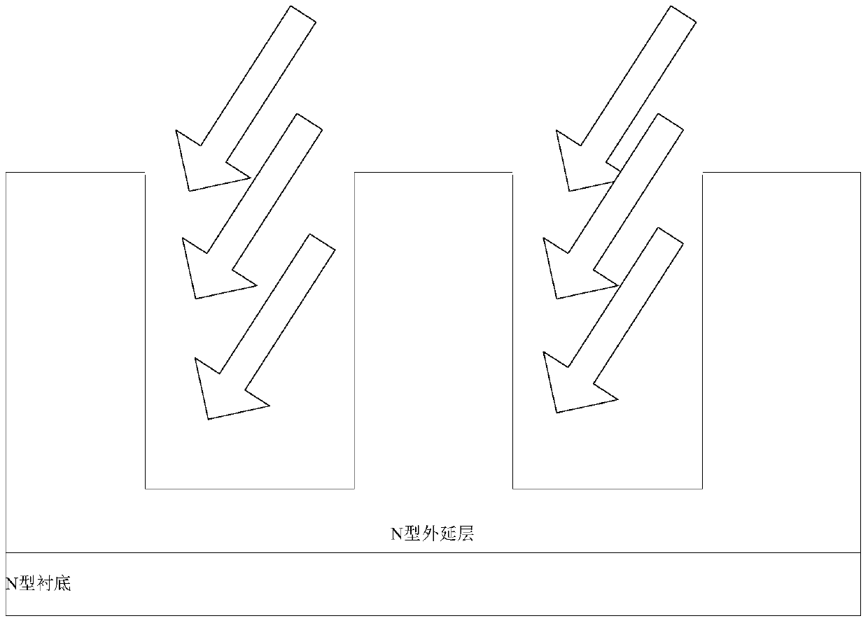
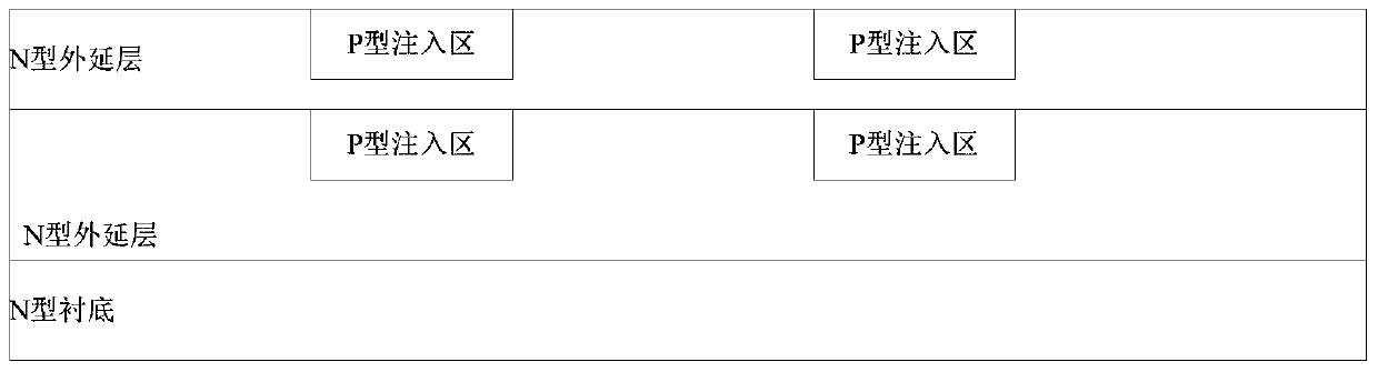
[0066] In order to save energy and reduce the power loss of the transistor, the on-resistance of the transistor should be reduced as much as possible; but because the breakdown voltage is proportional to the on-resistance, in order to solve this problem, a super-junction transistor, namely a super-junction MOSFET, is introduced. In order to improve the breakdown resistance characteristics of the device. Such as Figure 4 As shown, the embodiment of the present invention provides a super junction MOSFET structure, which specifically includes: a silicon substrate 1, a thick oxygen region 2, a diffusion column 3, a source region 4, a silicon body region 5, a gate oxide polycrystalline layer 6, a dielectric Layer 7 and metal layer 8. in,

[0067] A plurality of grooves are opened on the silicon substrate 1, and a thick oxygen region 2 is formed in the groove, and a diffusion column 3 is formed between the thick oxygen region 2 and the inner wall of the groove, and the doping typ...


PUM


Abstract

The invention discloses a super-junction MOSFET structure and a preparation method therefor. A deep-groove etching technology is adopted, so that complicated processes of multiple times of photoetching, ion implantation, epitaxial growth and the like in a conventional process are avoided, and the manufacturing cost is effectively lowered; and in addition, a thick oxygen region is grown in the super-junction MOSFET, so that the breakdown voltage of a device is effectively increased while conduction resistance is ensured at the same time.

Description

technical field [0001] The invention relates to the technical field of semiconductor chip manufacturing technology, in particular to a super junction MOSFET structure and a preparation method thereof. Background technique [0002] In order to save energy and reduce power loss in transistors such as those used in DC-to-DC converters, currently in MOSFET devices, power loss can be reduced by reducing the on-resistance of the device. However, the breakdown voltage of the MOSFET device is proportional to the on-resistance, and when the on-resistance decreases, the breakdown voltage will be adversely affected. In order to solve this problem, a super junction MOSFET is introduced, which includes alternating P-type regions and N-type regions located below the active region of the device. The alternating P-type regions and N-type regions in the super-junction MOSFET are ideally in a state of charge balance. , so that these regions deplete each other under reverse voltage conditions...

Claims


Application Information

Patent Timeline
Patent Type & Authority Patents(China)
IPC IPC(8): H01L29/06H01L29/78H01L21/336
Inventor 赵圣哲李理马万里
Owner FOUNDER MICROELECTRONICS INT
Features
  • R&D
  • Intellectual Property
  • Life Sciences
  • Materials
  • Tech Scout
  • Unparalleled Data Quality
  • Higher Quality Content
  • 60% Fewer Hallucinations
Learn More