OLED display panel and manufacturing method of OLED display panel

A technology for a display panel and a manufacturing method, which is applied to the manufacturing of semiconductor/solid-state devices, electrical components, and electrical solid-state devices, etc., can solve the problems of the influence of electron-hole recombination probability, the increase of uncontrollable factors, and the low utilization rate of materials, so as to improve the The effect of luminescent performance, improving film thickness compactness, and improving film thickness consistency

Inactive Publication Date: 2017-01-04
TCL CHINA STAR OPTOELECTRONICS TECH CO LTD
View PDF4 Cites 0 Cited by
  • Summary
  • Abstract
  • Description
  • Claims
  • Application Information

AI Technical Summary

Problems solved by technology

The scattering layer inside the device is generally prepared by evaporation, the material utilization rate is low, and its molecular structure will also have a great impact on the recombination probability of electrons and holes. The thickness of the device can cause changes in the film layer of the device, resulting in an increase in uncontrollable factors

Method used


Image

  • OLED display panel and manufacturing method of OLED display panel
  • OLED display panel and manufacturing method of OLED display panel
  • OLED display panel and manufacturing method of OLED display panel

Examples


Embodiment Construction

[0021] The following will clearly and completely describe the technical solutions in the embodiments of the present invention with reference to the accompanying drawings in the embodiments of the present invention. Obviously, the described embodiments are only some, not all, embodiments of the present invention. Based on the embodiments of the present invention, all other embodiments obtained by persons of ordinary skill in the art without creative efforts fall within the protection scope of the present invention.

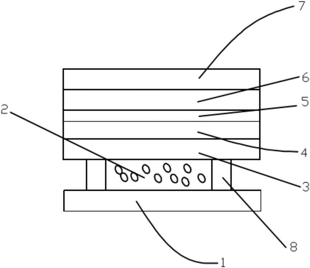
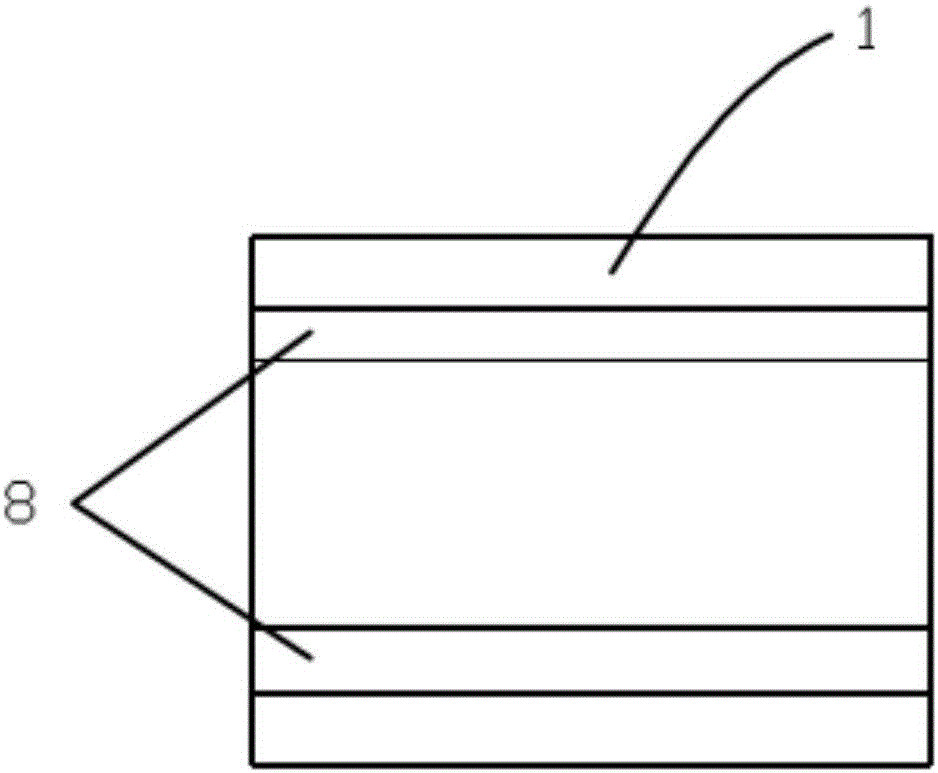
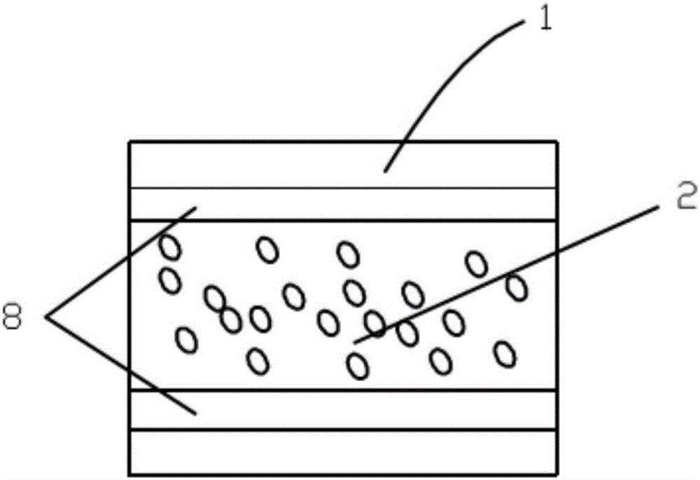
[0022] refer to figure 1 and Figure 2a , shows an OLED display panel according to the present invention, the OLED display panel includes a substrate 1, and a scattering layer 2, an anode 3, an organic functional layer 4, a light emitting layer 5, a cathode 6 and a cover plate 7 sequentially formed above the substrate 1, the scattering The layer 2 is located in the middle area surrounded by the partition wall 8. In this structure, when the driving voltage is appli...


PUM


Abstract

The invention provides an OLED display panel. The OLED display panel comprises a substrate, a first electrode, a partition wall and a scattering layer, wherein the partition wall is positioned between the substrate and the first electrode; and the scattering layer is formed on the substrate and is positioned in an area surrounded by the partition wall. According to the OLED display panel provided by the invention, the scattering efficiency of the scattering layer can be improved, so that the luminous efficiency can be strengthened, and the luminous performance is improved. The invention also provides a manufacturing method of the OLED display panel.

Description

technical field [0001] The invention relates to the field of display technology, in particular to an OLED display panel and a method for manufacturing the OLED display panel. Background technique [0002] In the current field of lighting and display, due to the characteristics of organic electroluminescence (OLED), such as low starting voltage, thinness, and self-luminescence, more and more researches are widely used in the development of lighting products and panel industries. In order to meet the requirements of low energy consumption, thinness and surface light source. [0003] At present, OLED emits light mainly through the recombination of excitons, and then exits from the light-emitting layer into the air. For general bottom-emitting OLED lighting devices, the path of light emission is: light-emitting layer-anode-substrate-air. After four paths, it can reach the human eyes incident in the air. [0004] The light exits from the light-emitting layer into the air. There...

Claims


Application Information

Patent Timeline
Patent Type & Authority Applications(China)
IPC IPC(8): H01L51/52H01L51/56H01L27/32
CPCH10K59/00H10K50/80H10K50/854H10K71/00
Inventor 黄辉
Owner TCL CHINA STAR OPTOELECTRONICS TECH CO LTD
Why Eureka
Try Eureka