Logic device configuration method and device

A technology of logic devices and configuration methods, applied in the field of communications, can solve the problems of complex design circuits, and achieve the effect of low interface requirements and saving interface resources

Inactive Publication Date: 2017-01-11
ZTE CORP
View PDF4 Cites 3 Cited by
  • Summary
  • Abstract
  • Description
  • Claims
  • Application Information

AI Technical Summary

Problems solved by technology

[0007] However, not all processing chips support the above access interfaces, and the design circuit is relatively complicated, which has a strong dependence on the stability of the CPU output clock and the frequency range of the clock.

Method used


Image

  • Logic device configuration method and device
  • Logic device configuration method and device
  • Logic device configuration method and device

Examples


Embodiment Construction

[0029] Hereinafter, the present invention will be described in detail with reference to the drawings and examples. It should be noted that, in the case of no conflict, the embodiments in the present application and the features in the embodiments can be combined with each other.

[0030] It should be noted that the terms "first" and "second" in the description and claims of the present invention and the above drawings are used to distinguish similar objects, but not necessarily used to describe a specific sequence or sequence.

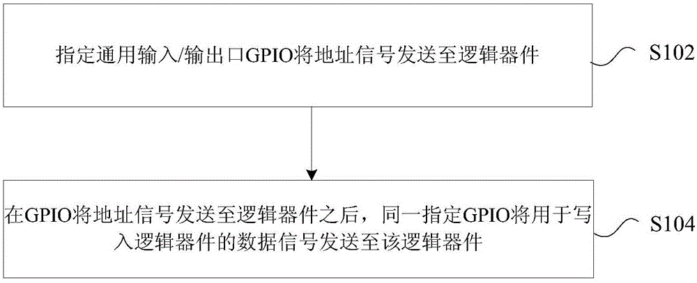
[0031] In this embodiment, a logic device configuration method is provided, figure 1 is a flowchart of a logic device configuration method according to an embodiment of the present invention, such as figure 1 As shown, the process includes the following steps:

[0032] Step S102, specifying the general-purpose input / output port GPIO to send an address signal to the logic device; wherein, the address signal is used to indicate the address of the logic...


PUM


Abstract

The invention provides a logic device configuration method and device, wherein the method comprises the following steps: an appointed universal input / output GPIO sends an address signal to a logic device, wherein the address signal is used for indicating the address of the logic device; and, after the GPIO sends the address signal to the logic device, the same appointed GPIO sends a data signal used for being written in the logic device to the logic device. By means of the logic device configuration method and device disclosed by the invention, the problems that a specific access interface needs to be used in a logic device configuration process and a design circuit is complex in the related technology can be solved; therefore, requirements of an interface provided by a CPU are low; and thus, interface resources are saved.

Description

technical field [0001] The present invention relates to the communication field, in particular to a logic device configuration method and device. Background technique [0002] General Purpose Input Output (GPIO) ports are widely used in embedded systems. Users can control the GPIO port to output high and low levels to transmit some signals through programming, which can be used as synchronization signals or control signals. [0003] Programmable logic devices are widely used in communication systems, and programs can be programmed in the following ways: [0004] Use JTAG tool / debugger for online programming; [0005] Use a dedicated chip burner to burn the bare chip offline; [0006] Use the data transfer interface provided by the device to program the device. Commonly used such as Local Bus bus interface, SPI bus interface; [0007] However, not all processing chips support the above access interfaces, and the design circuit is relatively complex, which has a strong dep...

Claims


Application Information

Patent Timeline
Patent Type & Authority Applications(China)
IPC IPC(8): G06F9/445G06F13/20
Inventor 刘佳妮
Owner ZTE CORP
Why Eureka
Try Eureka