Array substrate and preparation method thereof and display panel
A technology of array substrates and substrate substrates, which is applied in the manufacture of semiconductor/solid-state devices, the use of electromagnetic means, instruments, etc., can solve the problems of increasing the overall thickness of the display panel, and achieve the effect of solving the overall thickness increase and realizing temperature sensing
- Summary
- Abstract
- Description
- Claims
- Application Information
AI Technical Summary
Problems solved by technology
Method used
Image


Examples
Embodiment 1
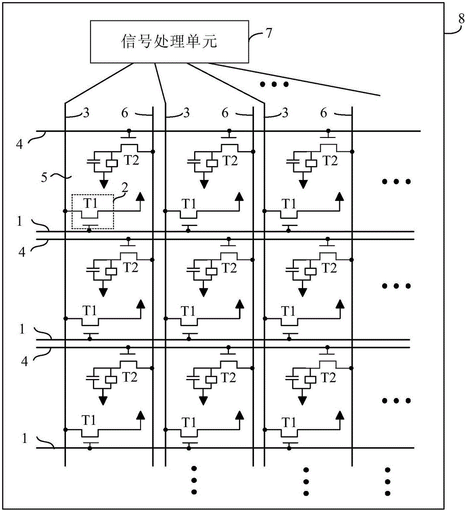
[0058] figure 1 A schematic structural diagram of an array substrate provided in Embodiment 1 of the present invention, as shown in figure 1 As shown, the array substrate includes: a base substrate 8 and a number of driving signal lines 1, a number of signal detection lines 3 and a number of temperature sensing modules 2 arranged on the base substrate 8, wherein the temperature sensing module 2 It is connected with the corresponding driving signal line 1 and signal detection line 3, the driving signal line 1 is used to output the driving signal to the temperature sensing module 2 to drive the temperature sensing module 2 to work, and the temperature sensing module 2 is used to sense the temperature , and output a corresponding current signal, and the signal detection line 3 is used to read the current signal output by the temperature sensing module 2 .
[0059] It should be noted that in the drawings, the drive signal line 1 extends horizontally, and the signal detection line...
Embodiment 2
[0072] image 3 It is a schematic structural diagram of an array substrate provided in Embodiment 2 of the present invention, Figure 4 for image 3 A cross-sectional schematic diagram of a pixel unit provided with a sensing thin film transistor and a temperature-sensitive resistor, as shown in image 3 and Figure 4 As shown, different from the first embodiment above, the temperature sensing module 2 in this embodiment not only includes the sensing thin film transistor T1, but also includes a temperature sensitive resistor St connected in series with the sensing thin film transistor T1.
[0073] Specifically, the first gate 9a of the sensing thin film transistor T1 is connected to the corresponding drive signal line 1, the first source 12a of the sensing thin film transistor T1 is connected to the first end of the temperature-sensitive resistor St, and the sensing thin film transistor T1 The first drain 13a of the sensor is connected to the corresponding signal detection l...
Embodiment 3
[0081] Figure 5 A schematic structural diagram of an array substrate provided in Embodiment 3 of the present invention, as shown in Figure 5 As shown, different from the array substrates in the first and second embodiments above, the driving signal line 1 and the gate line 4 in this embodiment are the same signal wiring.
[0082] Compared with the technical solutions of the first and second embodiments above, the technical solution provided by this embodiment can effectively reduce the number of signal traces on the array substrate, thereby helping to improve the aperture ratio.
[0083] In this embodiment, when the gate driving unit loads the driving signal to the gate line 4 (driving signal line 1) row by row, the display thin film transistor T2 and the temperature sensing module 2 (sensing thin film transistor T1) of the corresponding row are simultaneously activated. driving, the data signal in the data line 6 is written into the corresponding pixel electrode through th...
PUM
 Abstract
Description
Claims
Application Information