A Programmable Trimming Circuit of Output Port of Multiplexing Chip

An output port and circuit trimming technology, which is applied in the fields of logic circuit coupling/interface, logic circuit, logic circuit connection/interface layout, etc. using field effect transistors, can solve minor problems, save packaging costs and improve parameters The effect of precision and product yield

Active Publication Date: 2019-04-09
厦门芯一代集成电路有限公司
View PDF7 Cites 0 Cited by
  • Summary
  • Abstract
  • Description
  • Claims
  • Application Information

AI Technical Summary

Problems solved by technology

This method is simple to implement. For general products such as power management chips, the correction can be completed quickly and accurately. The impact of chip packaging on parameters is also small. However, products such as sensor chips are sensitive to packaging stress. Tuning reintroduces parameter deviations after packaging, so trimming during in-wafer test is of little value for this type of product

Method used


Image

  • A Programmable Trimming Circuit of Output Port of Multiplexing Chip
  • A Programmable Trimming Circuit of Output Port of Multiplexing Chip
  • A Programmable Trimming Circuit of Output Port of Multiplexing Chip

Examples


Embodiment Construction

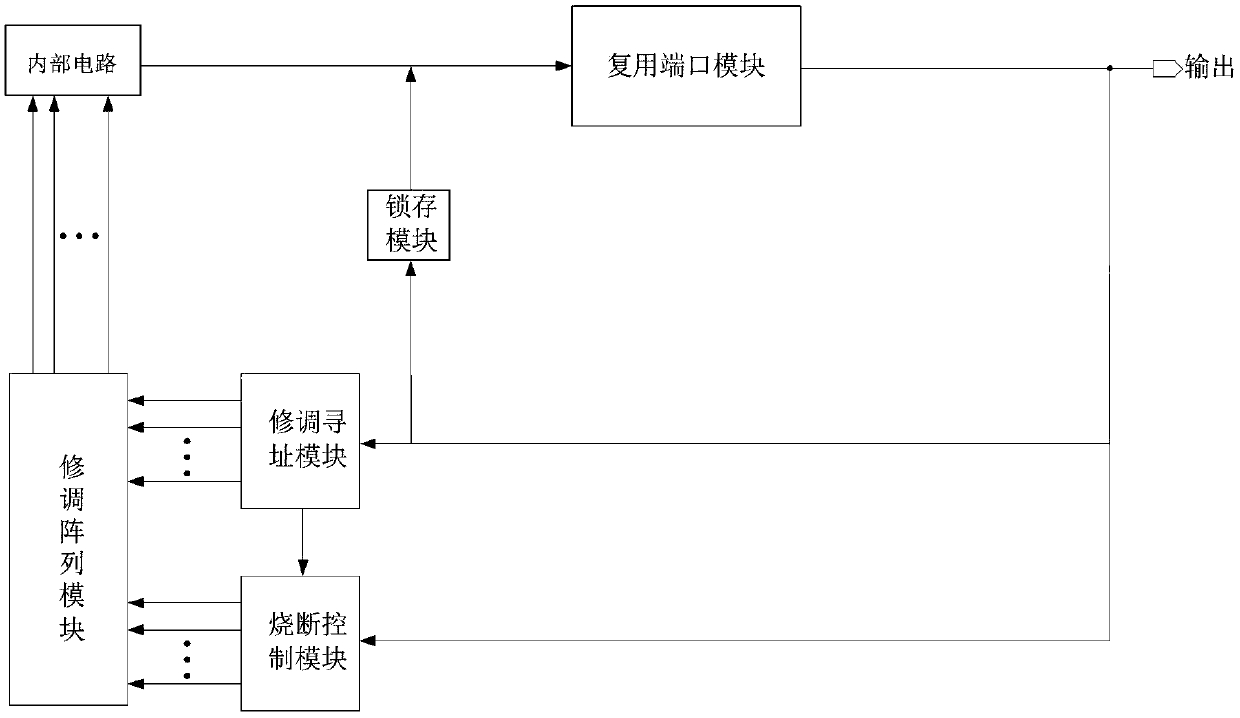
[0043] Such as figure 1 As shown, a programmable trimming circuit for output port of multiplexing chip, including internal circuit, multiplexing port module, latch module, trimming addressing module, burnout control module, trimming array module;

[0044] The internal circuit is the main circuit used to realize the function and performance of the chip, and the output terminal of the internal circuit is connected to the multiplexing port module;

[0045] The output ports of the multiplexing port module are respectively connected to the latch module, the trimming addressing module and the burnout control module, and are used to multiplex the output port of the chip as a trimming input port for outputting addressing signals and blown out signals , and respectively transmit the addressing signal to the latch module and the trimming addressing module, and transmit the blown signal to the blown control module;

[0046] The output terminal of the latch module is connected to the out...


PUM


Abstract

The invention discloses a programmable trimming circuit multiplexing a chip output port. The programmable trimming circuit comprises an internal circuit, a port multiplexing module, a latch module, a trimming addressing module, a burn control module and a trimming array module; in view of the limitation of the trimming mode of a measurement link in a wafer, a trimming method of a chip finished product test link is provided for multiplexing an output end as a programmable trimming port without increasing the chip port, therefore the packaging cost can be reduced, and meanwhile the parameter precision and the product yield of specific chips sensitive to packaging stress are also improved.

Description

technical field [0001] The invention relates to the field of integrated circuits, in particular to a programmable trimming circuit for multiplexing chip output ports. Background technique [0002] In the field of integrated circuit product manufacturing, due to the deviation of the process, there is often a deviation between the design value of the chip parameter and the test value of the actual finished product, especially the key parameters with high precision requirements, so it needs to be adjusted according to the test value of the chip , in order to make key parameters meet the expected design requirements and improve product yield. [0003] The more commonly used trimming method is the mid-wafer testing link in the chip production process. According to the test results at this stage, the parameters that do not meet the requirements are trimmed to the required values ​​by laser blowing or voltage fusing before entering the chip package. links. This method is simple t...

Claims


Application Information

Patent Timeline
Patent Type & Authority Patents(China)
IPC IPC(8): H03K19/0185
CPCH03K19/018507
Inventor 姜帆陈利刘玉山
Owner 厦门芯一代集成电路有限公司
Why Eureka
Try Eureka