Eureka AIR delivers breakthrough ideas for toughest innovation challenges, trusted by R&D personnel around the world.

Array substrate, method for manufacturing array substrate, and display device

A technology for array substrates and display devices, which is applied in nonlinear optics, instruments, optics, etc., can solve the problems of low flatness of array substrates, and achieve the effect of high flatness

Active Publication Date: 2020-11-24
BOE TECH GRP CO LTD +1
View PDF14 Cites 0 Cited by
  • Summary
  • Abstract
  • Description
  • Claims
  • Application Information

AI Technical Summary

Problems solved by technology

[0005] In order to solve the problem of low flatness of the array substrate in the related art, an embodiment of the present invention provides an array substrate, a method for manufacturing the array substrate, and a display device

Method used


Image

  • Array substrate, method for manufacturing array substrate, and display device
  • Array substrate, method for manufacturing array substrate, and display device
  • Array substrate, method for manufacturing array substrate, and display device

Examples


Embodiment Construction

[0059] In order to make the object, technical solution and advantages of the present invention clearer, the implementation manner of the present invention will be further described in detail below in conjunction with the accompanying drawings.

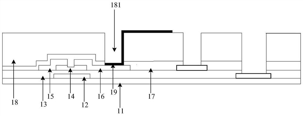
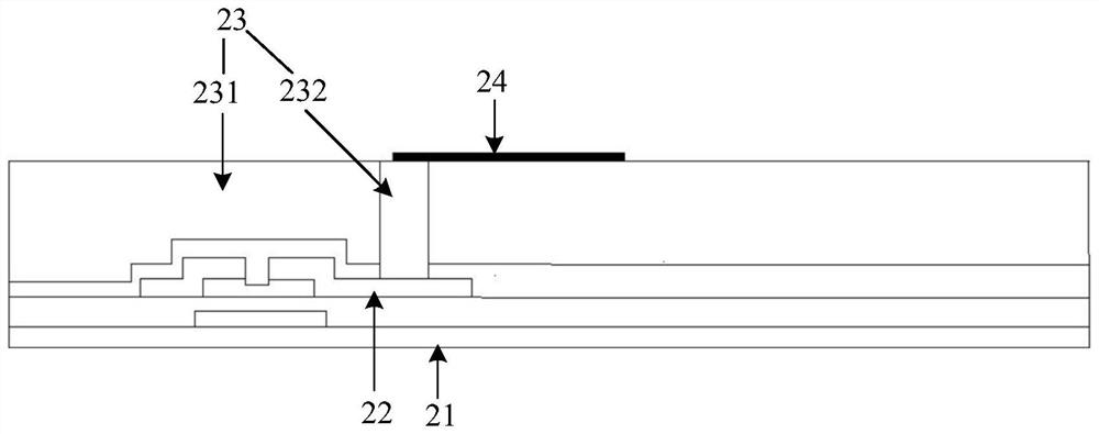
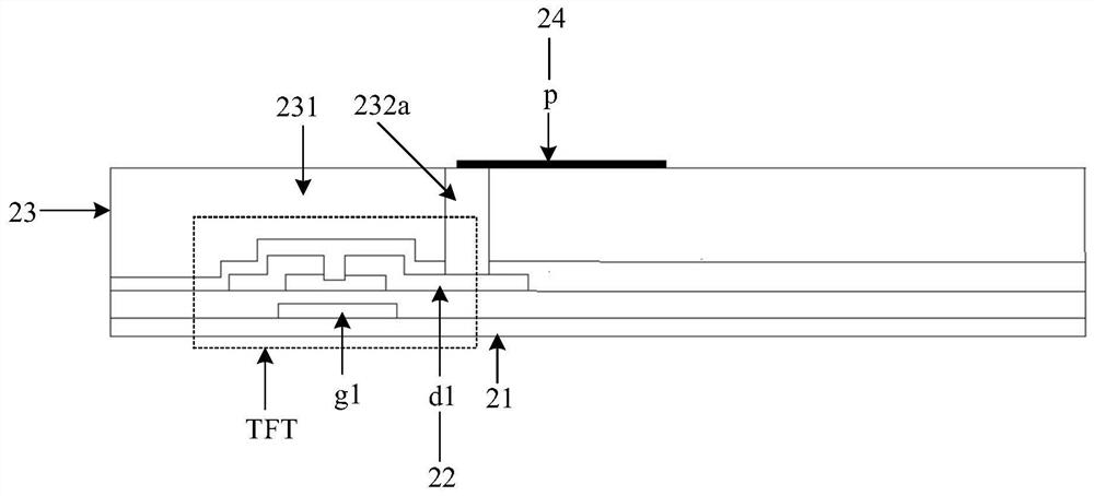
[0060] An embodiment of the present invention provides an array substrate, such as figure 2 As shown, the base substrate 21; the base substrate 21 is provided with at least one electrode 22; the base substrate 21 provided with at least one electrode 22 is provided with a resin layer 23; the base substrate 21 provided with the resin layer 23 is provided with There is at least one electrode 24 . Wherein, the resin layer 23 includes an insulating region 231 and at least one conductive region 232, and each conductive region 232 is respectively connected to two electrodes ( figure 1 Shown is that electrode 22 and electrode 23 need to be in contact.

[0061] There are usually multiple electrodes on the upper and lower sides of the resin l...


PUM


Abstract

The invention discloses an array substrate, a manufacturing method thereof and a display device and belongs to the technical field of display. The array substrate comprises a substrate base plate, wherein at least one electrode are arranged on the substrate base plate; a resin layer is arranged on the substrate base plate where at least one electrode are arranged; at least one electrode are arranged on the substrate base plate where the resin layer is arranged; the resin layer comprises an insulating area and at least one conductive area, and each conductive area is separately in contact with two electrodes which are located at the upper and lower sides of the corresponding conductive area and required to be in conduction. According to the array substrate provided by the invention, the electrodes at the two sides of the resin layer are connected through the conductive areas in the resin layer, so that the problems in related technologies that when the electrodes above the insulating area are connected with the electrodes below the insulating area through via holes of the insulating area, relatively large depressions will be formed at the via holes of the insulating area, and the flatness of the array substrate is relatively low are solved. The effect that the flatness of the array substrate is relatively high is achieved.

Description

technical field [0001] The present invention relates to the field of display technology, in particular to an array substrate, a method for manufacturing the array substrate, and a display device. Background technique [0002] Thin Film Transistor Liquid Crystal Display (TFT-LCD for short) has the characteristics of small size, low power consumption, and high picture quality, and occupies a dominant position in the display market. The performance parameter of TFT-LCD is the main determinant factor that determines that the liquid crystal display is superior to other display modes, and the aperture ratio is a performance parameter to measure the light utilization rate of the liquid crystal display. The higher the aperture ratio, the brightness of the display screen. The higher the value, the lower the energy consumption of the display. [0003] At present, an organic resin can be used to increase the aperture ratio of the TFT-LCD. The organic resin can effectively reduce the c...

Claims


Application Information

Patent Timeline
Patent Type & Authority Patents(China)
IPC IPC(8): G02F1/1343
CPCG02F1/134309
Inventor 操彬彬马骏钱海蛟
Owner BOE TECH GRP CO LTD
Why Eureka
Eureka Blog
Learn More