Pattern recognition device and electronic equipment

A technology of electronic equipment and devices, which is applied in the field of pattern recognition devices and electronic devices, can solve the problems that the relative position of valleys and ridges cannot be judged, the accuracy of fingerprint recognition devices is affected, and the light energy attenuation is attenuated.

Inactive Publication Date: 2017-01-25
BOE TECH GRP CO LTD
View PDF5 Cites 41 Cited by
  • Summary
  • Abstract
  • Description
  • Claims
  • Application Information

AI Technical Summary

Problems solved by technology

[0003] Usually, the light emitted by the backlight source 12 is divergent, that is, two adjacent light rays will be farther and farther apart after propagating. After multiple diffuse reflections, the finger print is reached. At this time, the energy of the light is severely attenuated. When the energy of the li...

Method used


Image

  • Pattern recognition device and electronic equipment
  • Pattern recognition device and electronic equipment
  • Pattern recognition device and electronic equipment

Examples


Embodiment Construction

[0036] The following will clearly and completely describe the technical solutions in the embodiments of the present invention with reference to the accompanying drawings in the embodiments of the present invention. Obviously, the described embodiments are only some, not all, embodiments of the present invention.

[0037] In addition, the terms "first" and "second" are used for descriptive purposes only, and cannot be understood as indicating or implying relative importance or implicitly specifying the quantity of indicated technical features. Thus, a feature defined as "first" and "second" may explicitly or implicitly include one or more of these features. In the description of the present invention, unless otherwise specified, "plurality" means two or more.

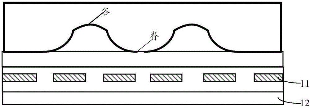
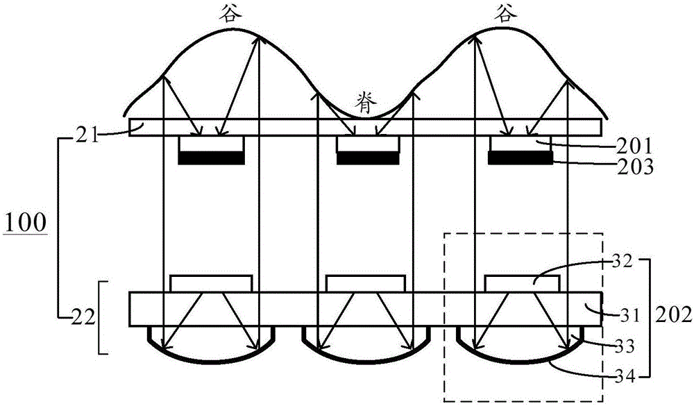
[0038] The present invention provides a texture recognition device, comprising a first base substrate and a backlight structure arranged oppositely, the first substrate substrate is located on the light emitting side of ...


PUM


Abstract

An embodiment of the invention provides a pattern recognition device and electronic equipment and relates to the technical field of display with an aim to improve accuracy in pattern recognition. The pattern recognition device can be applied to fingerprint recognition process. The pattern recognition device comprises a first substrate and a backlit structure which are arranged on an opposite manner, the first substrate is located on the light dipping side of the backlit structure, the surface, deviating from the backlit structure, of the first substrate is provided with a pattern collecting surface, and multiple photoelectric sensors are arranged on the first substrate; the backlit structure is used for giving out collimated light, and the collimated light, after sent out from the pattern collecting surface of the first substrate, is reflected to the photoelectric sensors via patterns.

Description

technical field [0001] The invention relates to the field of display technology, in particular to a texture recognition device and electronic equipment. Background technique [0002] Such as figure 1 As shown, the optical fingerprint identification device is generally provided with a plurality of photoelectric sensors 11, such as photodiodes and phototransistors. The backlight 12 is a surface light source, and the light emitted by the backlight 12 is diffusely reflected after it hits the finger. Part of the light will be received by the photoelectric sensor 11, and the photoelectric sensor 11 will convert the received light signal into a corresponding electrical signal, and the light will be reflected when it passes through the trough (hereinafter referred to as valley) and peak (hereinafter referred to as ridge) of the finger print, The light energy of reflected light will vary. Generally, the light energy reflected by the valley is lower than the light energy reflected b...

Claims


Application Information

Patent Timeline
IPC IPC(8): G06K9/00
CPCG06V40/1359G06V40/1324G02F1/13338G02F1/133605G02F1/133606
Inventor 谭纪风
Owner BOE TECH GRP CO LTD
Why Eureka
Try Eureka