Flash memory and manufacturing method thereof

A manufacturing method and memory technology, applied in the field of semiconductors, can solve the problems of easy interference and unreliable performance of flash memory, etc., and achieve the effect of avoiding mutual interference

Active Publication Date: 2017-01-25
SEMICON MFG INT (SHANGHAI) CORP
View PDF4 Cites 11 Cited by
  • Summary
  • Abstract
  • Description
  • Claims
  • Application Information

AI Technical Summary

Problems solved by technology

[0004] However, as the size of flash memory cells decreases, the distance between adjacent flash memory cells becomes smaller, and int

Method used


Image

  • Flash memory and manufacturing method thereof
  • Flash memory and manufacturing method thereof
  • Flash memory and manufacturing method thereof

Examples


Embodiment Construction

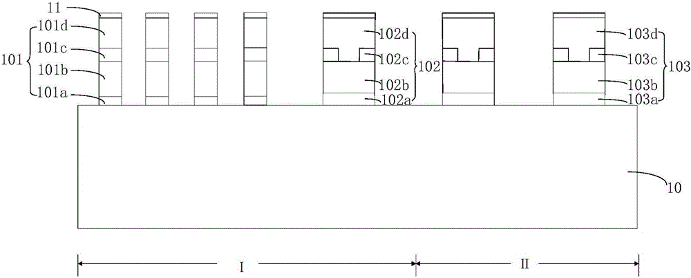
[0034] As mentioned in the background technology, in the prior art, as the size decreases, the distance between adjacent flash memory cells becomes smaller, and interference between the two is prone to occur when reading, writing, and erasing, which will cause poor performance of the flash memory. reliable. After analysis, the inventor found that the reason for this is: in order to electrically insulate the gate stack structure of adjacent flash memory cells, a dielectric layer is filled between the two, and the material of the above dielectric layer is generally silicon dioxide, which causes During the charging and discharging process of read, write, and erase operations, the parasitic capacitance is too large, so the unoperated cells are prone to be disturbed and change their storage status.

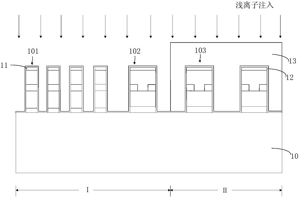
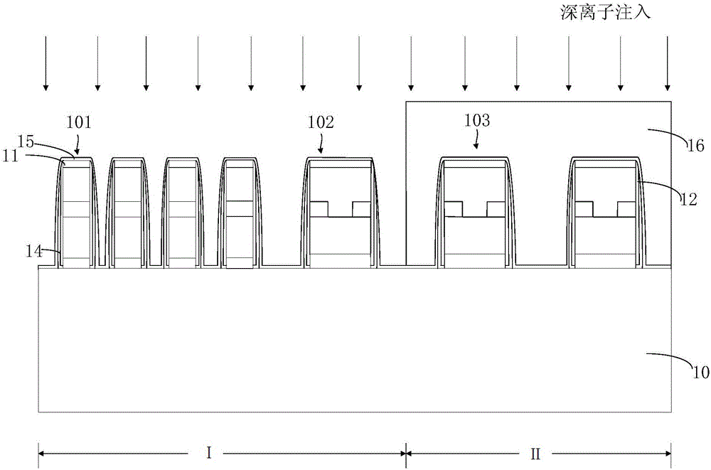
[0035] Based on the above analysis, the present invention forms an air gap between the gate stack structures of adjacent flash memory cells to reduce parasitic capacitance and avoid in...


PUM


Abstract

The invention relates to a flash memory and a manufacturing method thereof. The flash memory and the manufacturing method thereof have the advantages that during the filling of the grid stack structure of adjacent memory transistors, a filling process with poor filling performance is used so as to form an air gap between the adjacent memory transistors, the dielectric constant of the air gap is smaller than that of a silicon dioxide dielectric layer, and accordingly stray capacitance generated during reading, writing and erasing can be reduced, and mutual interference between the adjacent transistors is avoided.

Description

technical field [0001] The invention relates to the technical field of semiconductors, in particular to a flash memory and a manufacturing method thereof. Background technique [0002] In the current semiconductor industry, integrated circuit products can be mainly divided into three types: analog circuits, digital circuits and digital / analog hybrid circuits, among which storage devices are an important type of digital circuits. In recent years, among storage devices, the development of flash memory (flash memory) is particularly rapid. The main feature of flash memory is that it can keep stored information for a long time without power on, so it is widely used in various memories that need to store data that will not disappear due to power interruption, and that need to be read and written repeatedly. Moreover, flash memory has the advantages of high integration, fast access speed, easy erasing and rewriting, etc., so it has been widely used in many fields such as micro-el...

Claims


Application Information

Patent Timeline
IPC IPC(8): H01L27/11517
Inventor 仇圣棻孔繁生
Owner SEMICON MFG INT (SHANGHAI) CORP
Why Eureka
Try Eureka