

Tooling for chip cutting experiment and method
A chip and experimental technology, applied in the manufacturing of electrical components, electric solid-state devices, semiconductor/solid-state devices, etc., can solve the problems of poor manual cutting accuracy, slow speed, high cost, etc. flexible effects
- Summary
- Abstract
- Description
- Claims
- Application Information
AI Technical Summary
Problems solved by technology
Method used
Image

Examples
Embodiment Construction
[0032] The principles and features of the present invention are described below in conjunction with the accompanying drawings, and the examples given are only used to explain the present invention, and are not intended to limit the scope of the present invention.
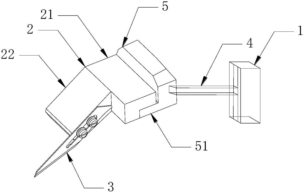
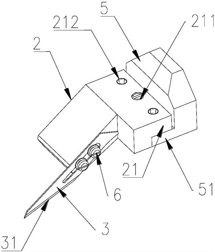
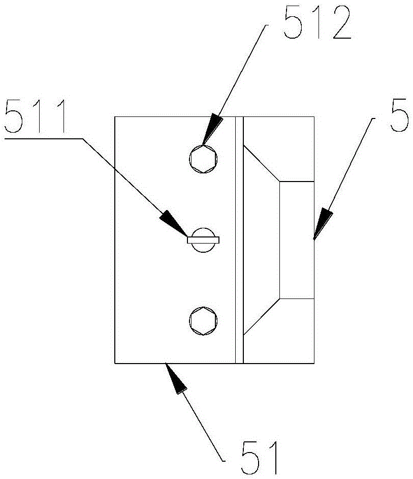
[0033] Such as figure 1 Or as shown in 2, a kind of tooling that is used for the chip cutting experiment of this embodiment, in the chip cutting experiment, the wafer is cut into a chip or the chip is cut, including a microwave probe station, a connector 2 and a cutting blade 3; The probe station includes a base 1 and a mechanical displacement device slidingly connected to the base 1. The other end of the mechanical displacement device is fitted with one end of the connector 2 for driving the connector 2 to move. The cutting blade 3 It is fixedly installed with the other end of the connector 2, and the cutting blade 3 is located above the wafer or chip to be cut.
[0034] The microwave probe station in this embodim...
PUM
 Abstract
Description
Claims
Application Information