Driving method of image sensor
A technology of an image sensor and a driving method, which is applied in the direction of image communication, color TV parts, TV system parts, etc., and can solve problems such as poor image quality
- Summary
- Abstract
- Description
- Claims
- Application Information
AI Technical Summary
Problems solved by technology
Method used
Image
Examples
Embodiment 1
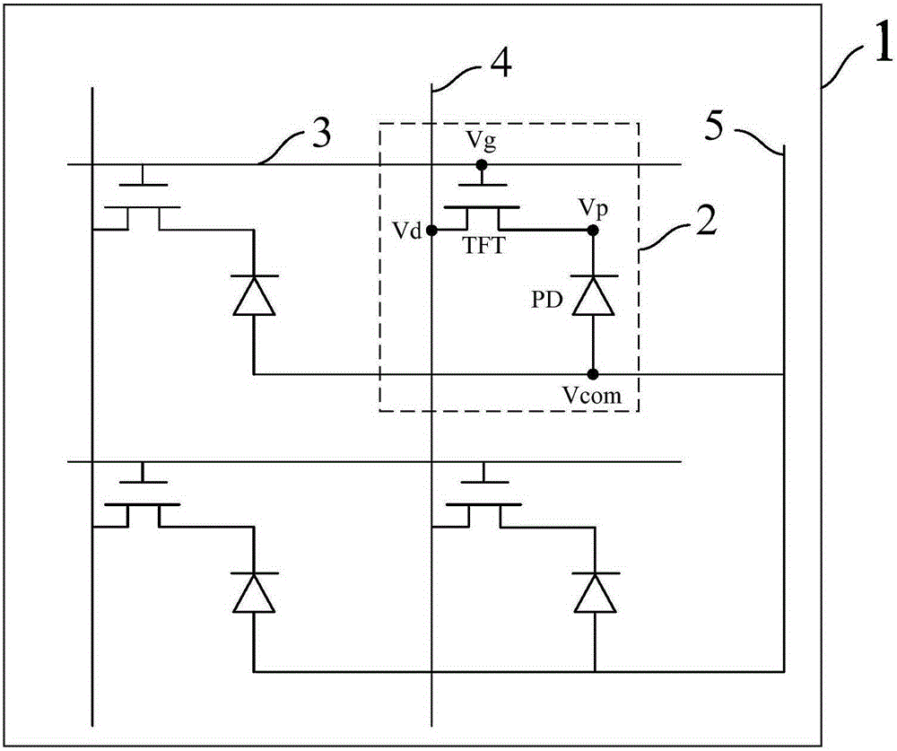
[0050] Such as figure 1 Shown is a schematic structural view of a flat panel detector, which includes pixel units 2 arranged in a two-dimensional array. In this embodiment, the pixel units 2 form an array of 2 rows and 2 columns. The pixel unit 2 includes a switch element and a photodiode PD. In this embodiment, the switch element is a thin film transistor TFT. The cathode of the photodiode PD is connected to the source of the thin film transistor TFT as a pixel electrode; the gates of the thin film transistors TFT located in the same row are connected to the same scanning line 3, and the gates of the thin film transistor TFT located in the same column The drains are connected to the same data line 4 , and the anodes of the photodiodes PD are connected to the common electrode 5 .
[0051] Such as Figure 4 Shown is the relationship between the source-drain current Ids and the gate-source voltage Vgs of a conventional N-type amorphous silicon thin film transistor (the figure...
Embodiment 2
[0064] The first embodiment takes an N-type thin film transistor as an example, and this method is also applicable to a P-type switching element. In this embodiment, a P-type thin film transistor is taken as an example, and its principle is basically the same as that of the embodiment, except that the N-type thin film transistor is replaced by a P-type thin film transistor.
[0065] The conduction characteristics of the P-type thin film transistor are as follows: when VgsVth, the thin film transistor is in an off state. In this embodiment, the potential Vcom of the common electrode 5 is a positive potential, taking 8V as an example.
[0066] Reset phase: the switching element is turned on by reducing the gate voltage of the switching element to perform a reset operation.
[0067] Waiting for exposure stage: reducing the gate potential of the switching element to a set potential, at which time the switching element is still in the off state, and the set potential is lower than...
PUM
 Abstract
Description
Claims
Application Information


