Evaluation method for bulk silicon carbide single crystals and reference silicon carbide single crystal used in said method

一种碳化硅单晶、评价方法的技术,应用在通过测量材料受应力时其光学性质的变化力的计量、材料激发分析、力/扭矩/功测量仪等方向,能够解决再现性不充分、晶格常数差、晶格常数不同等问题

Active Publication Date: 2017-02-15
RESONAC CORPORATION
View PDF16 Cites 10 Cited by
  • Summary
  • Abstract
  • Description
  • Claims
  • Application Information

AI Technical Summary

Problems solved by technology

[0009] However, in the case of this patent document 3, in addition to the difference in lattice constant between the sapphire substrate and GaN, stretching is caused by the difference in lattice constant between the n-type GaN layer, the light emitting layer, and the p-type GaN layer. Stress, since lattice strain occurs due to this tensile stress, it is considered that evaluation using Raman shift is possible
That is, the difference between the frequency of Raman scattered light and the frequency of incident light (Raman shift) is very small after all, and it is difficult to evaluate the lattice strain in a single SiC single crystal
In addition to Patent Document 3, there have been reported examples in which the periphery of the titanium silicide pattern and Stress distribution around the device isolation film (see Non-Patent Document 1), but it is considered that a large stress of 150 to 350 MPa acts on the Si substrate around the titanium silicide pattern, and it is still in a state where a large lattice strain is induced determination
[0010] In addition, the Raman shift is easily affected by fluctuations in the wavelength of the laser light of the Raman spectrometer used in the measurement and the thermal strain of the measuring device, and the reproducibility of the measurement is insufficient.
Therefore, even if the Raman shift can be measured in principle or research, it is not suitable for evaluating the lattice strain of single crystal monomers in industrial production applications.

Method used


Image

  • Evaluation method for bulk silicon carbide single crystals and reference silicon carbide single crystal used in said method
  • Evaluation method for bulk silicon carbide single crystals and reference silicon carbide single crystal used in said method
  • Evaluation method for bulk silicon carbide single crystals and reference silicon carbide single crystal used in said method

Examples


Embodiment 1

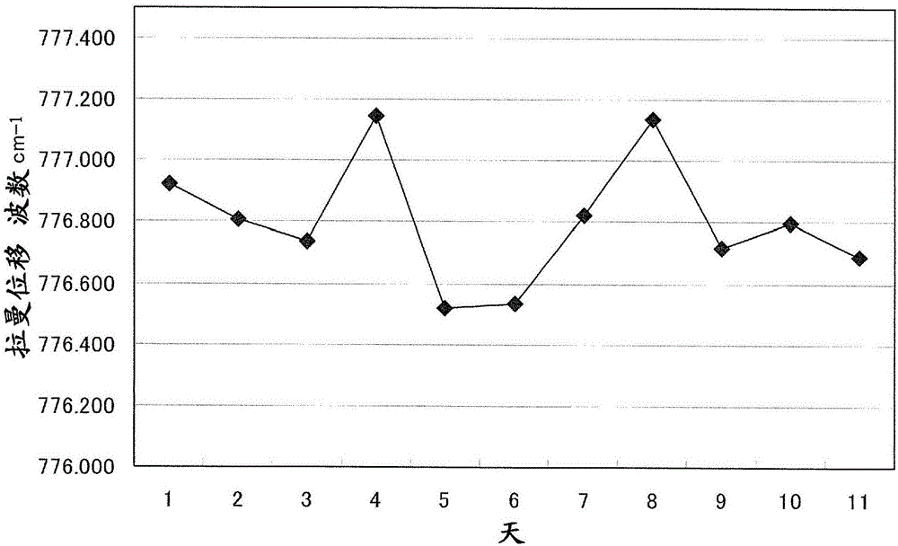
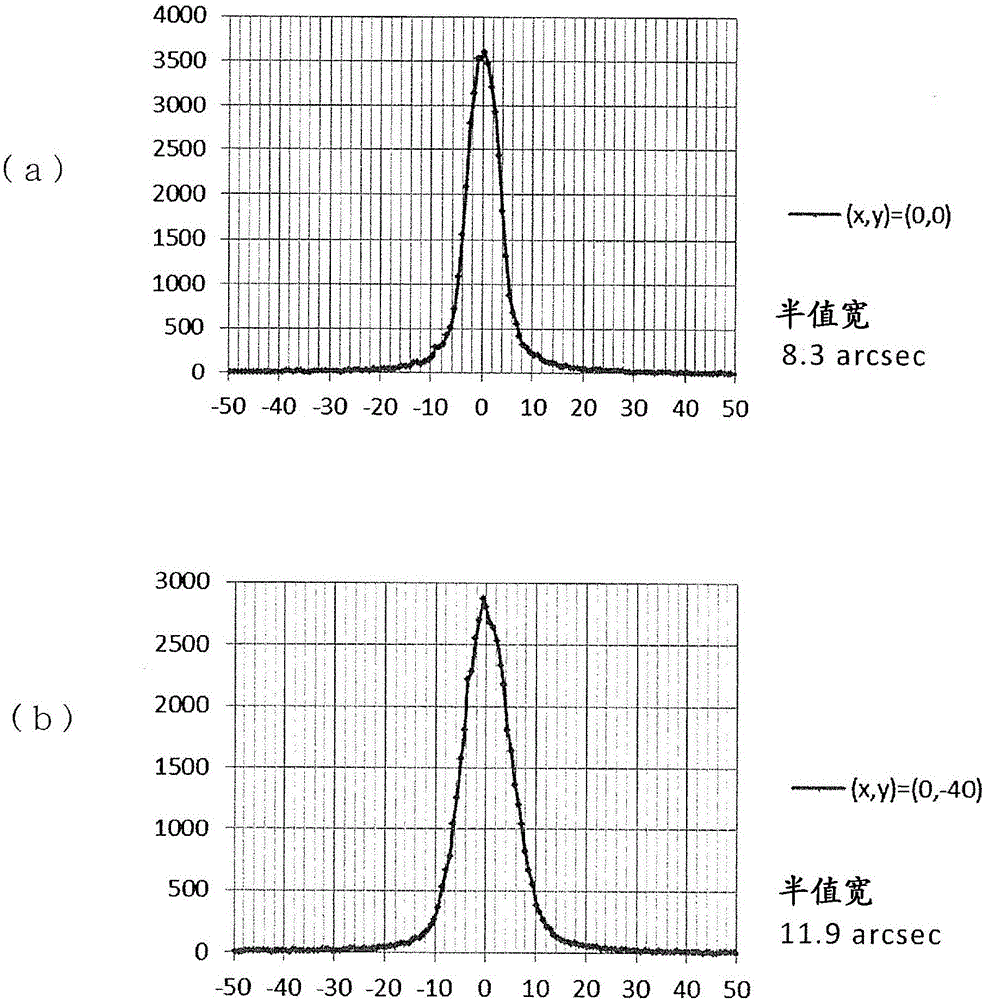
[0052] First, a 2-inch (diameter 55 mm) 4H-type SiC single crystal ingot manufactured by the sublimation recrystallization method was ground, cut into a thickness of 0.5 mm using a multi-wire saw, polished to a thickness of 0.36 mm by diamond polishing, and finally Chemical mechanical polishing (CMP) thereby processes the substrate. The surface roughness Ra was set at 0.1 nm. Then, a 10 mm square piece was cut out from the center of the substrate to obtain a SiC single crystal for reference with a thickness of 0.35 mm and a size of 10 mm×10 mm. Furthermore, a SiC single crystal ingot of the reference SiC single crystal was obtained, and the nitrogen concentration was 6×10 18 ~9×10 18 atom / cm 3 , In addition, observation of etch pits was carried out by molten alkali etching near the obtained reference SiC single crystal, and the result was that the dislocation density was 4.8×10 3 / cm 2 , 0.6 microtubules / cm 2 . Furthermore, an X-ray rocking curve was measured for a wafe...

Embodiment 2

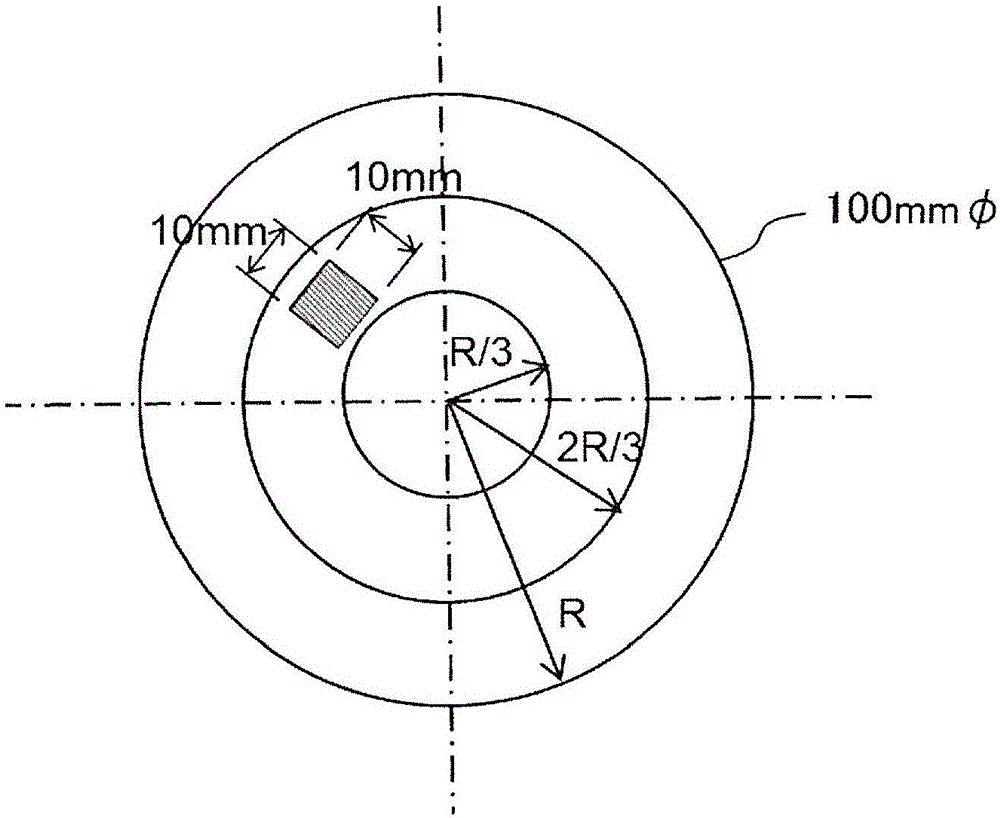
[0062] A 4-inch (diameter 105 mm) 4H-type SiC single crystal ingot manufactured by the sublimation recrystallization method is ground and cut into a thin plate with a thickness of 2 mm using a multi-wire saw, and the center part of the radius connecting the center and the circumference is cut. A 15mm square piece was cut out. In this Example 2, a slightly thick sheet was made in consideration of handleability. Next, the Si surface and the C surface were polished together by diamond polishing to obtain a reference SiC single crystal having a surface roughness Ra of 0.3 nm, a thickness of 1.9 mm, and a size of 15 mm×15 mm. Furthermore, a SiC single crystal ingot of the reference SiC single crystal was obtained, and the nitrogen concentration was 4.0×10 19 atom / cm 3 , In addition, the observation of corrosion pits was carried out by molten alkali etching near the obtained reference SiC single crystal, and the dislocation density was 3.7×10 3 / cm 2 , 0.3 microtubules / cm 2 . ...


PUM

PropertyMeasurementUnit
roughnessaaaaaaaaaa
sizeaaaaaaaaaa
band gapaaaaaaaaaa

Abstract

The purpose of the present invention is to provide a method that makes it possible to relatively evaluate the degree of lattice distortion in a plurality of bulk SiC single crystals, and a reference SiC single crystal used in said method. Provided is a bulk silicon carbide single crystal evaluation method for relatively evaluating the lattice distortion magnitudes of a plurality of bulk silicon carbide single crystals under evaluation by measuring the Raman shift (Rref) in a reference silicon carbide single crystal used as a standard, measuring the Raman shifts (Rn) of each of the plurality of bulk silicon carbide single crystals under evaluation, determining the differences between each of the Raman shifts (Rn) and the Raman shift (Rref), and comparing the differences to each other. Also provided is a reference silicon carbide single crystal that is used in said method and has a square shape with sides between 5 mm and 50 mm in length, a thickness between 100 [mu]m and 2000 [mu]m, a surface roughness (Ra) of 1 nm or less, a micro-pipe density of 1.0 / cm<2> or less, and a dislocation density of 5 * 103 / cm<2> or less.

Description

technical field [0001] The present invention relates to a method for evaluating bulk silicon carbide single crystals and a reference silicon carbide single crystal used in the method. An evaluation method of bulk silicon carbide single crystals for relatively evaluating the magnitude of strain of their crystal lattices by spectroscopic methods, and a reference silicon carbide single crystal used in this method. Background technique [0002] Silicon carbide (SiC) is a wide bandgap semiconductor having a wide band gap of 2.2 to 3.3 eV, and due to its excellent physical and chemical properties, it is being researched and developed as an environment-resistant semiconductor material. Especially in recent years, it has attracted attention as a material for short-wavelength optical devices from blue to ultraviolet, high-frequency electronic devices, high-voltage high-output electronic devices, etc., including power semiconductors. Devices using SiC (semiconductor elements) ) resea...

Claims


Application Information

Patent Timeline
Patent Type & Authority Applications(China)
IPC IPC(8): G01N21/65
CPCG01L5/0047G01N21/65G01L1/24
Inventor 小岛清中林正史
Owner RESONAC CORPORATION
Why Eureka
Try Eureka