Three-dimensional Trench Electrode Silicon Detector with Variable Central Collecting Electrode
A collection electrode and center electrode technology, applied in circuits, electrical components, semiconductor devices, etc., can solve the problems of large impact on radiation resistance, inconvenient adjustment of volume, uneven electric field distribution, etc. Adjusting inconvenient and practically enhanced effects
- Summary
- Abstract
- Description
- Claims
- Application Information
AI Technical Summary
Problems solved by technology
Method used
Image
Examples
Embodiment 1
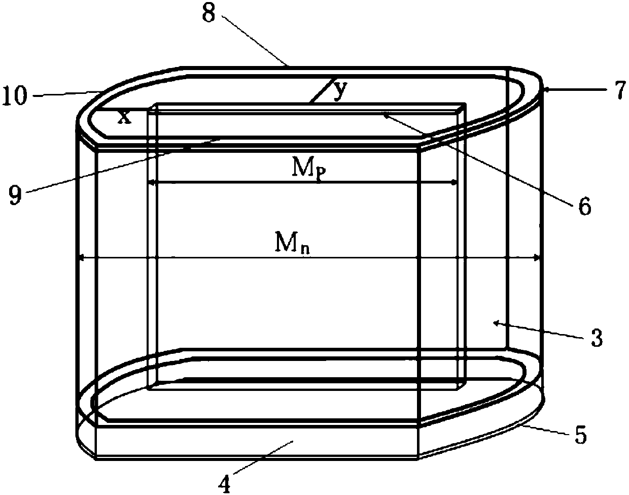
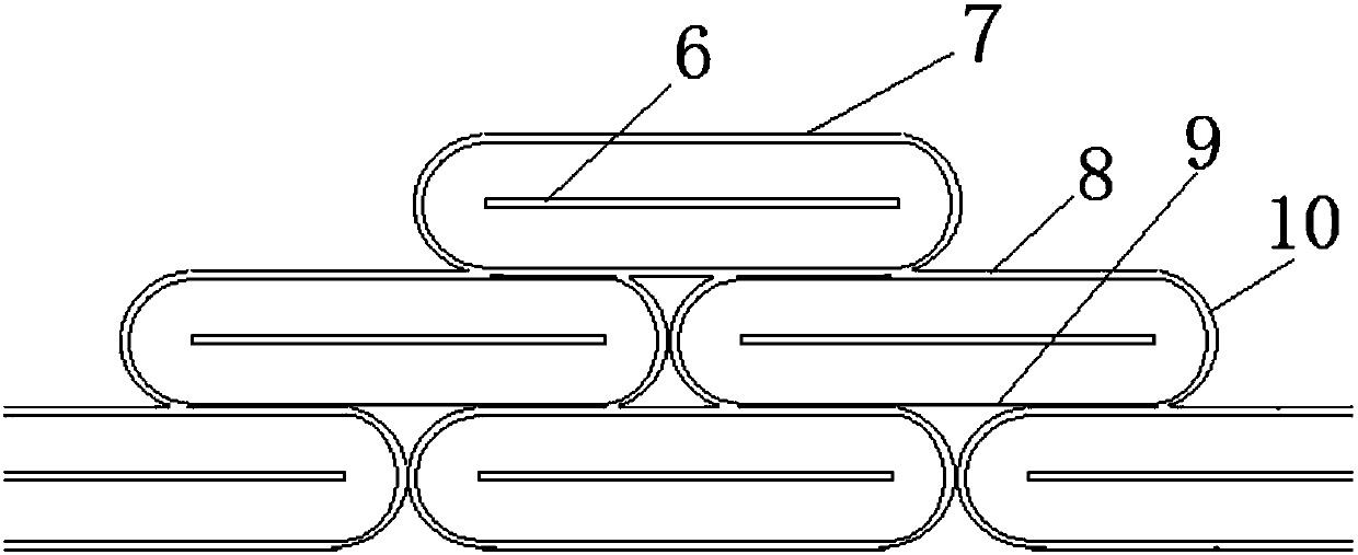
[0021] The structure of the present invention, such as Figure 2-3 As shown, the peripheral electrode 7 is composed of a first straight part 8, a second straight part 9 and a curved part 10, the first straight part 8 and the second straight part 9 are parallel, and the end of the first straight part 8 and the second straight part The ends of the two straight parts 9 are closed and connected by a curved part 10, and the curved part 10 is preferably semicircular; the long central electrode 6 is located in the middle of the peripheral electrode 7, and the long central electrode 6 is connected to the first straight part 8 and the second straight part. 9 in parallel, there is an isolated silicon body 3 between the peripheral electrode 7 and the long central electrode 6, and the p-type silicon substrate 4 is placed under the peripheral electrode 7 and the long central electrode 6, and the bottom of the p-type silicon substrate 4 is plated with a 1 μm-thick two-layer silicon substrate...
Embodiment 2
[0024] In the structure of the present invention, except that the thickness of the heavily doped borosilicate layer and the heavily doped phosphorus silicon layer is 500 μm, the thickness of the lightly doped borosilicate layer is 500 μm, and the thickness of the p-type silicon substrate 4 is 20 μm, the remaining parts are the same as those in the embodiment. 1 is the same.
Embodiment 3
[0026] In the structure of the present invention, except that the thickness of the heavily doped borosilicate layer and the heavily doped phosphorus silicon layer is 270 μm, the thickness of the lightly doped borosilicate layer is 270 μm, and the thickness of the p-type silicon substrate 4 is 30 μm, the remaining parts are the same as those in the embodiment. 1 is the same.
[0027] Considering that the positive electrode is located in the center of the traditional three-dimensional trench electrode silicon detector, its breakdown voltage is significantly reduced, while the long center electrode 6 of the present invention makes the position of the positive and negative electrodes different, and the impact on the breakdown voltage is relatively reduced, and the long The central electrode 6 changes with the change of the peripheral electrode 7, that is, M p with M n match (M n -M p =2y), where M p Indicates the length of the long center electrode 6, M nIndicates the length ...
PUM
 Abstract
Description
Claims
Application Information


