Pressure sensor and packaging method thereof

A pressure sensor and packaging method technology, applied in piezoelectric/electrostrictive/magnetostrictive devices, decorative arts, electric solid devices, etc., can solve the problem of sensitive film damage, large peripheral stress of the sensitive film, difficult to effectively prevent the sensitive film Damage and other problems to achieve the effect of extending the service life and enhancing the overall protection performance

Active Publication Date: 2018-07-31
MEMSENSING MICROSYST SUZHOU CHINA
View PDF8 Cites 0 Cited by
  • Summary
  • Abstract
  • Description
  • Claims
  • Application Information

AI Technical Summary

Problems solved by technology

[0003] The pressure sensor chip based on the above-mentioned sensitive film has the following problems when it is used to measure the contact stress: one is that the thickness of the sensitive film is small, usually set to tens of microns or even thinner, when directly measuring the pressure exerted by the human body, especially the finger, The force is directly transmitted to the sensitive membrane, which is easy to cause damage to the sensitive membrane
Second, when the pressure sensor chip is packaged, wires are required to achieve electrical connection, and the wires are usually set beyond the sensitive film. In the case of improper protection, it is easy to damage the wires
For example, Chinese patent CN101337652 A discloses a pressure sensor packaging structure, which transmits external stress through a flexible material arranged on the surface of the sensitive area, and protects the pad and lead wire through a hard material, but the flexible material is arranged on the surface of the sensitive film, and the sensitive film is in contact with the flexible material. The peripheral stress of the material bonding surface is relatively large, and it is difficult to effectively prevent the sensitive film from being damaged; and the process is relatively complicated and the volume is large

Method used


Image

  • Pressure sensor and packaging method thereof
  • Pressure sensor and packaging method thereof
  • Pressure sensor and packaging method thereof

Examples


Embodiment Construction

[0037] The present invention will be described in detail below with reference to the embodiments shown in the accompanying drawings. However, this embodiment does not limit the present invention, and any structural, method, or functional changes made by those skilled in the art according to this embodiment are included in the protection scope of the present invention.

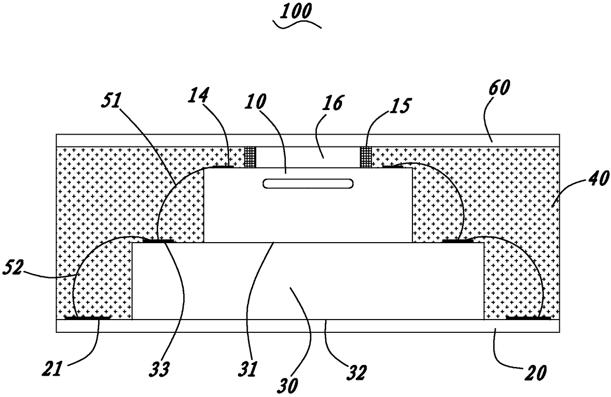
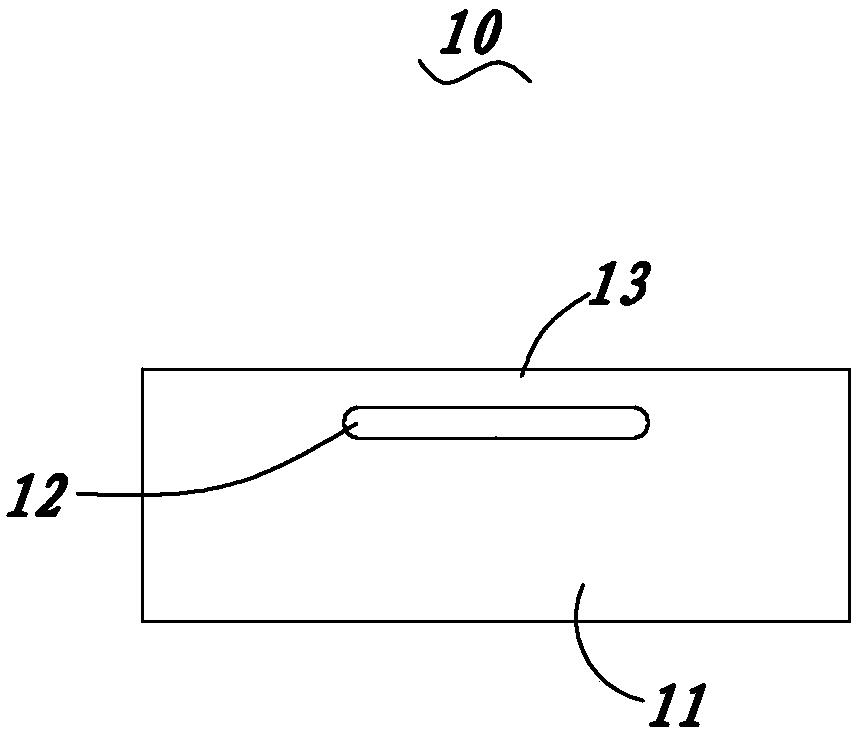
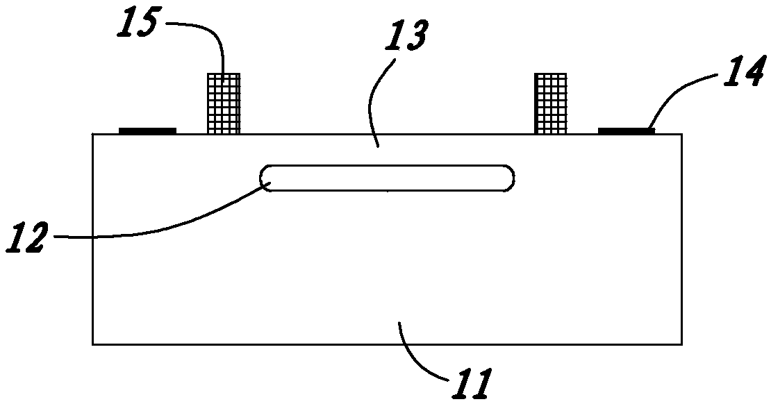
[0038] refer to Figure 1 to Figure 5 Shown is a preferred embodiment of the pressure sensor 100 of the present invention. The pressure sensor 100 provided by the present invention includes a stacked pressure sensor chip 10 and a substrate 20, the pressure sensor chip 10 includes a substrate 11, a cavity 12 formed on the side of the substrate 11 away from the substrate 20, and the The cavity 12 cooperates with the provided sensitive membrane 13 . The cavity 12 is flat; the first pad 14 is provided on the substrate 11 .

[0039] Preferably, the first pad 14 is made by using processes such as deposition, photo...


PUM


Abstract

The present invention provides a pressure sensor and a packaging method thereof. The pressure sensor includes a laminated substrate and a pressure sensor chip. The pressure sensor chip includes a substrate, a cavity formed on the side of the substrate away from the substrate, and A sensitive film arranged in cooperation with the cavity, the cavity is flat, a first pad is provided on the substrate; a second pad electrically connected to the first pad is provided on the substrate; The pressure sensor also includes a first dam arranged along the outer periphery of the sensitive membrane, a hard sealing layer arranged on the substrate and not exceeding the first dam, and a dam located above the sensitive membrane and connected to the The pressure-bearing part abutting against the first dam, wherein the first welding pad is located outside the first dam. By adopting the pressure sensor and its packaging method of the present invention, the sensitive film is prevented from being directly subjected to external stress, the probability of damage is reduced, and at the same time, better protection is achieved through the hard sealing layer, and the service life is prolonged.

Description

technical field [0001] The invention relates to the technical field of micro-electro-mechanical systems, in particular to a pressure sensor and a packaging method thereof. Background technique [0002] At this stage, various consumer electronics products such as mobile phones, tablet computers, toys, remote controls, etc. pay more and more attention to intelligent development and human-computer interaction design, which also makes the market demand for pressure sensors that sense the contact stress of the human body, especially fingers. increasing day by day. At the same time, higher performance requirements are also put forward for this type of pressure sensor. First, it is necessary to effectively transmit the external stress to the sensitive film of the pressure sensor chip. Second, it is necessary to protect the sensitive film and lead wires on the chip from being damaged. Finally, In order to meet the trend of increasingly miniaturized portable consumer electronics, it...

Claims


Application Information

Patent Timeline
Patent Type & Authority Patents(China)
IPC IPC(8): B81B7/02B81C1/00H01L23/31
CPCH01L23/3107B81B7/02B81C1/00261B81C1/00269B81C1/00325B81B2201/02H01L2924/181H01L2224/16225H01L2224/48091H01L2224/48145H01L2924/00014H01L2924/00012
Inventor 胡维吕萍李刚
Owner MEMSENSING MICROSYST SUZHOU CHINA
Why Eureka
Try Eureka