
Manufacturing method of mask structure
A manufacturing method and mask technology, applied in semiconductor/solid-state device manufacturing, electrical components, circuits, etc., can solve the problems that the mask is easy to be stained with particles or impurities, affect the quality of the mask, and achieve the effect of improving quality
- Summary
- Abstract
- Description
- Claims
- Application Information
AI Technical Summary
Problems solved by technology
Method used
Image

Examples
Embodiment Construction
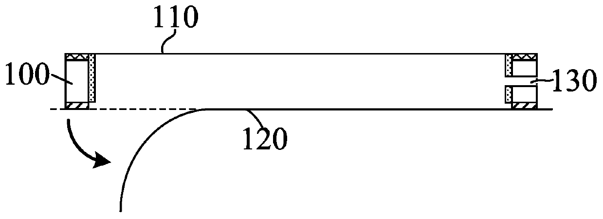
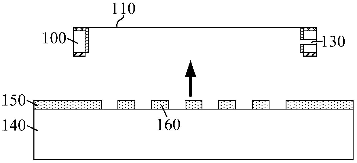
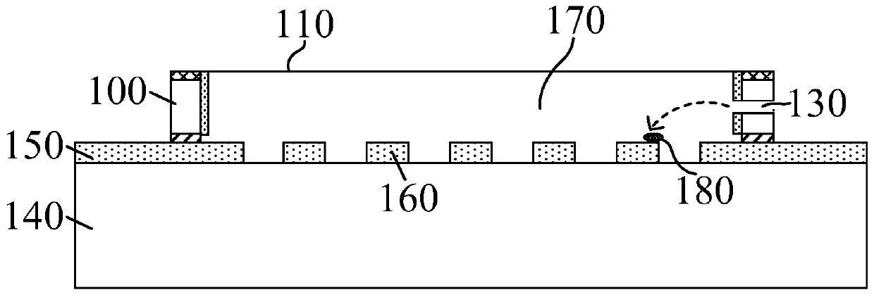
[0031] The mask plate manufactured by the prior art is easy to be stained with particles or impurities during use, combined with Figure 1 to Figure 3 Analyzing the reason why the mask is contaminated, in the mask manufacturing process, mainly includes: providing a mask and protective film device 100, the mask includes a substrate 140 and a patterned metal layer on the substrate 140; The protective film device 100 includes a protective film 110 at the top of the device, and a bracket positioned below the protective film 110. An opening 130 is formed in the side wall of one side of the bracket for separating the air pressure in the protective film device 100 from the outside world. The air pressure of the environment is the same; after the sealing tape 120 of the protective film is torn off, the substrate 140 is directly adhered to the protective film device 100, so that the patterned metal layer is in contact with the bracket to form a protective film 110. The mask plate, the p...
PUM
 Abstract
Description
Claims
Application Information