Shift register and driving method thereof, gate driving circuit, and display device

A shift register and driving signal technology, applied in static memory, digital memory information, instruments, etc., can solve problems such as abnormal display, keeping low potential, and unstable pull-up nodes

Active Publication Date: 2017-03-15
BOE TECH GRP CO LTD
View PDF5 Cites 15 Cited by
  • Summary
  • Abstract
  • Description
  • Claims
  • Application Information

AI Technical Summary

Problems solved by technology

[0004] Embodiments of the present invention provide a shift register, its driving method, a gate driving circuit and a display device, which are used to solve the problem that in the prior art, in the low potential holding stage, the pull-up node cannot stably maintain low potential, thereby causing shift The output of the drive signal output terminal of the bit register produces noise, which may even cause abnormal display problems

Method used


Image

  • Shift register and driving method thereof, gate driving circuit, and display device
  • Shift register and driving method thereof, gate driving circuit, and display device
  • Shift register and driving method thereof, gate driving circuit, and display device

Examples


Embodiment 1

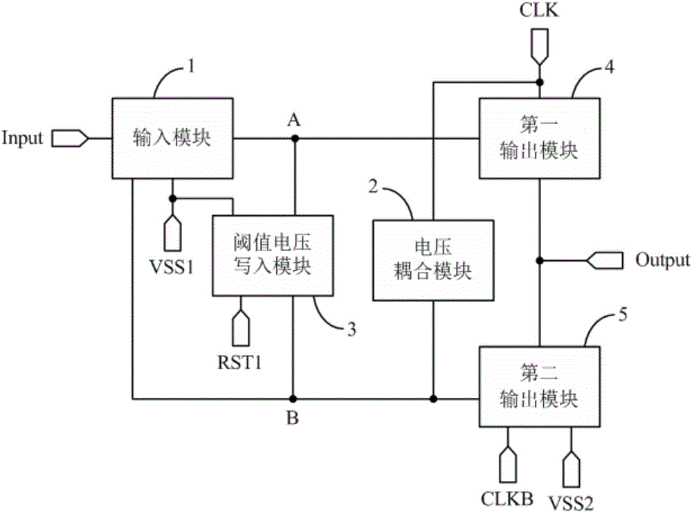
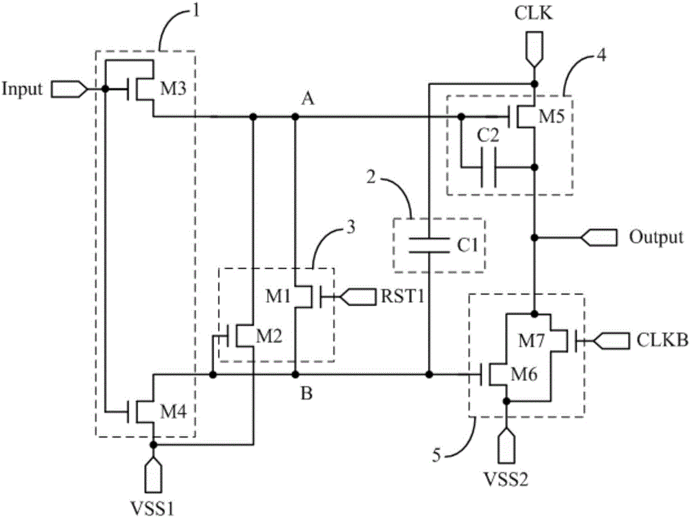
[0108] by Figure 2a The structure of the shift register shown is taken as an example to describe its working process, wherein, in Figure 2a In the shift register shown, all the switch transistors are N-type switch transistors, and each N-type switch transistor is turned on under the action of a high potential, and is turned off under the action of a low potential; the potential of the first reference signal terminal VSS1 is a low potential, The corresponding input and output timing diagrams are as follows Figure 3a Shown, specifically, select as Figure 3a There are six stages in the shown input-output timing diagram: the first stage T1 , the second stage T2 , the third stage T3 , the fourth stage T4 , the fifth stage T5 and the sixth stage T6 .

[0109] In the first stage T1, Input=1, RST1=0, CLK=0, CLKB=1.

[0110] Since Input=1, both the third switch transistor M3 and the fourth switch transistor M4 are turned on. Since the third switching transistor M3 is turned on ...

Embodiment 2

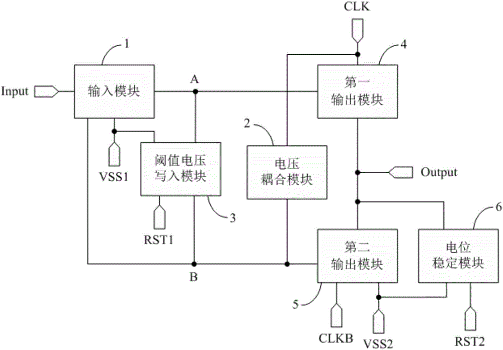
[0123] by Figure 2b The structure of the shift register shown is taken as an example to describe its working process, wherein, in Figure 2bIn the shift register shown, all the switch transistors are N-type switch transistors, and each N-type switch transistor is turned on under the action of a high potential, and is turned off under the action of a low potential; the potential of the first reference signal terminal VSS1 is a low potential, The corresponding input and output timing diagrams are as follows Figure 3b Shown, specifically, select as Figure 3b There are six stages in the shown input-output timing diagram: the first stage T1 , the second stage T2 , the third stage T3 , the fourth stage T4 , the fifth stage T5 and the sixth stage T6 .

[0124] In the first stage T1, Input=1, RST1=0, RST2=0, CLK=0, CLKB=1. Since RST2=0, the eighth switching transistor M8 is turned off. The rest of the specific working process is the same as the working process of the first stag...


PUM


Abstract

The invention discloses a shift register and a driving method thereof, a gate driving circuit, and a display device. The shift register comprises an input module, a voltage coupling module, a threshold voltage writing module, a first output module, and a second output module. Through cooperation of the four modules, the voltage of a second node can be compensated, so that the potential of a first node can be kept in a steady state of invalid potential after the shift register outputs an effective pulse signal of a driving signal. Therefore, the output noise at a driving signal output end is reduced, and abnormal display is avoided.

Description

technical field [0001] The invention relates to the field of display technology, in particular to a shift register, a driving method thereof, a gate driving circuit and a display device. Background technique [0002] With the rapid development of display technology, the display panel is more and more developed towards the direction of high integration and low cost. Among them, the gate driver on array (Gate Driver on Array, GOA) technology integrates the thin film transistor (Thin Film Transistor, TFT) gate switching circuit on the array substrate of the display panel to form a scan drive for the display panel, so that the gate driver can be omitted. The wiring space of the Bonding area of ​​the integrated circuit (Integrated Circuit, IC) and the fan-out (Fan-out) area can not only reduce the product cost in terms of material cost and manufacturing process, but also enable the display panel to achieve Beautiful design with symmetry on both sides and narrow frame; moreover, ...

Claims


Application Information

Patent Timeline
Patent Type & Authority Applications(China)
IPC IPC(8): G09G3/36G09G3/3266G11C19/28
CPCG09G3/3266G09G3/3677G09G2320/0219G11C19/28
Inventor 韩明夫商广良韩承佑金志河姚星郑皓亮袁丽君王志冲
Owner BOE TECH GRP CO LTD
Why Eureka
Try Eureka