Manufacturing method of image sensor

An image sensor and manufacturing method technology, applied in the direction of electric solid-state devices, semiconductor devices, radiation control devices, etc., can solve the problems of inability to sense, limit the application range of sensors, etc., and achieve the effect of avoiding solder ball occlusion and preventing electromagnetic interference

Inactive Publication Date: 2017-03-15
南通沃特光电科技有限公司
View PDF7 Cites 0 Cited by
  • Summary
  • Abstract
  • Description
  • Claims
  • Application Information

AI Technical Summary

Problems solved by technology

The sensor can only sense the light on the front side, but not the light on the back side, which limits the application range of the sensor

Method used


Image

  • Manufacturing method of image sensor
  • Manufacturing method of image sensor
  • Manufacturing method of image sensor

Examples


no. 1 example

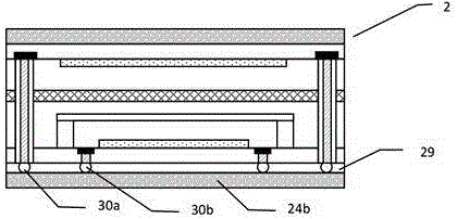
[0029] see figure 2 , an anti-interference image sensor 2, comprising:

[0030] A first substrate 21a, which may be a silicon substrate, on which electronic components (light receiving regions) are formed, the first substrate 21a includes a front surface having a first light receiving region 22a and a rear surface opposite to the front surface ;

[0031] A silicon substrate 31, the silicon substrate 31 comprising a front with a groove 25 and a back opposite to the front, the depth of the groove 25 is small, the thickness of the silicon substrate 31;

[0032] The second substrate 21b is arranged at the bottom of the groove 25, the second substrate 21b includes a front with a second light receiving area 22b and a back opposite to the front, the front of the second substrate 21b Coplanar with the back surface of the silicon substrate 31, the bottom of the groove 25 should be far away from the first light receiving region 22a;

[0033] The back side of the first substrate 21 a...

no. 2 example

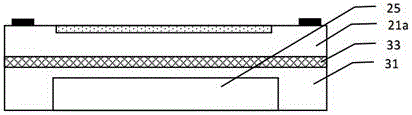
[0053] see image 3 , an anti-interference image sensor 3, comprising:

[0054] A first substrate 21a, which may be a silicon substrate, on which electronic components (light receiving regions) are formed, the first substrate 21a includes a front surface having a first light receiving region 22a and a rear surface opposite to the front surface ;

[0055] A silicon substrate 31, the silicon substrate 31 comprising a front with a groove 25 and a back opposite to the front, the depth of the groove 25 is small, the thickness of the silicon substrate 31;

[0056] The second substrate 21b is arranged at the bottom of the groove 25, the second substrate 21b includes a front with a second light receiving area 22b and a back opposite to the front, the front of the second substrate 21b Coplanar with the back surface of the silicon substrate 31, the bottom of the groove 25 should be far away from the first light receiving region 22a;

[0057] The back side of the first substrate 21 a ...


PUM


Abstract

The invention provides a manufacturing method of an image sensor. The method comprises the steps that (1) a first substrate is provided, wherein the first substrate comprises a front surface with a first light receiving area and a back surface opposite to the front surface; (2) a silicon substrate is provided, wherein the silicon substrate comprises a front surface with a groove and a back surface opposite to the front surface; (3) the back surface of the first substrate and the front surface of the silicon substrate are bonded through an iron-cobalt alloy layer; and (4) a second substrate is provided, the second substrate is arranged at the bottom of the groove and comprises a front surface with a second light receiving area and a back surface opposite to the front surface, and the front surface of the second substrate and the back surface of the silicon substrate are coplanar.

Description

technical field [0001] The invention relates to the sensor field of sensitive components, in particular to a manufacturing method of an anti-interference image sensor. Background technique [0002] The simplest electronic device in the photosensitive sensor is the photoresistor, which can sense the light and dark changes of the light, output a weak electrical signal, and control the automatic switch of the LED lamp through simple electronic circuit amplification. Therefore, it is widely used in automatic control and household appliances. For remote lighting fixtures, such as: automatic brightness adjustment in TVs, automatic exposure in cameras; Stop device and anti-theft alarm device Medium [0003] Photosensitive sensor is one of the most common sensors. It has a wide variety, mainly including: photocell, photomultiplier tube, photoresistor, phototransistor, solar cell, light sensor, ultraviolet sensor, fiber optic photoelectric sensor, color sensor, CCD and CMOS image s...

Claims


Application Information

Patent Timeline
Patent Type & Authority Applications(China)
IPC IPC(8): H01L27/146H01L23/552
CPCH01L27/14685H01L23/552H01L27/14623H01L27/14636H01L27/14683
Inventor 王汉清
Owner 南通沃特光电科技有限公司
Why Eureka
Try Eureka