A method of manufacturing a sensor

A manufacturing method and sensor technology, which are used in the manufacture of microstructure devices, piezoelectric devices/electrostrictive devices, and processes for producing decorative surface effects, can solve problems such as limiting the application range of sensors and inability to sense, and achieve Eliminate the circuit board, avoid occlusion, and ensure the effect of thinning

Active Publication Date: 2017-11-07
山东鸿荣电子有限公司
View PDF8 Cites 0 Cited by
  • Summary
  • Abstract
  • Description
  • Claims
  • Application Information

AI Technical Summary

Problems solved by technology

The sensor can only sense the light on the front side, but not the light on the back side, which limits the application range of the sensor

Method used


Image

  • A method of manufacturing a sensor
  • A method of manufacturing a sensor
  • A method of manufacturing a sensor

Examples


no. 1 example

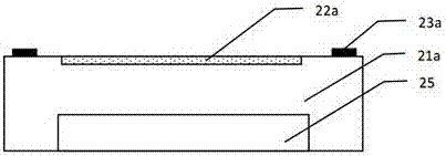
[0028] see figure 2 , a double-sided image sensor 2 comprising:

[0029] A first substrate 21a, which may be a silicon substrate, on which electronic components (light receiving regions) are formed, the first substrate 21a includes a front surface having a first light receiving region 22a and a rear surface opposite to the front surface ;

[0030] The groove 25 on the back side of the first substrate 21a, the depth of the groove 25 is less than or equal to half the thickness of the first substrate, and the bottom of the groove 25 should be far away from the first light receiving area 22a;

[0031] The second substrate 21b fixed on the bottom of the groove 25, the second substrate 21b includes a front with a second light receiving area 22b and a back opposite to the front, the front of the second substrate 21b coplanar with the back surface of the first substrate 21a.

[0032] On the front side of the first substrate 21a, there is a first optical filter 24a bonded by a fir...

no. 2 example

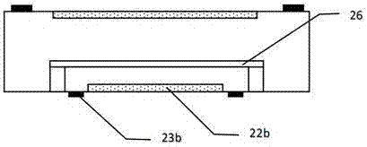
[0050] see image 3 , a double-sided image sensor 3 comprising:

[0051] A first substrate 21a, which may be a silicon substrate, on which electronic components (light receiving regions) are formed, the first substrate 21a includes a front surface having a first light receiving region 22a and a rear surface opposite to the front surface ;

[0052] The groove 25 on the back side of the first substrate 21a, the depth of the groove 25 is less than or equal to half the thickness of the first substrate, and the bottom of the groove 25 should be far away from the first light receiving area 22a;

[0053] The second substrate 21b fixed on the bottom of the groove 25, the second substrate 21b includes a front with a second light receiving area 22b and a back opposite to the front, the front of the second substrate 21b coplanar with the back surface of the first substrate 21a.

[0054] On the front side of the first substrate 21a, there is a first optical filter 24a bonded by a first ...


PUM


Abstract

The invention provides a manufacturing method of a sensor. The manufacturing method comprises the following steps: (1) providing a first substrate, wherein the first substrate comprises a front side provided with a first light receiving area and a back side opposite to the front side; (2) forming a groove in a back side of the first substrate, wherein the depth of the groove is smaller than or equal to a half of the thickness of the first substrate; and (3) providing a second substrate, and fixing the second substrate in the groove, wherein the second substrate comprises a front side provided with a second light receiving area and a back side opposite to the front side, and the front side of the second substrate and the back side of the first substrate are coplanar.

Description

technical field [0001] The invention relates to the sensor field of sensitive components, in particular to a manufacturing method of the sensor. Background technique [0002] The simplest electronic device in the photosensitive sensor is the photoresistor, which can sense the light and dark changes of the light, output a weak electrical signal, and control the automatic switch of the LED lamp through simple electronic circuit amplification. Therefore, it is widely used in automatic control and household appliances. For remote lighting fixtures, such as: automatic brightness adjustment in TVs, automatic exposure in cameras; Stop device and anti-theft alarm device Medium [0003] Photosensitive sensor is one of the most common sensors. It has a wide variety, mainly including: photocell, photomultiplier tube, photoresistor, phototransistor, solar cell, light sensor, ultraviolet sensor, fiber optic photoelectric sensor, color sensor, CCD and CMOS image sensor, etc. Major dome...

Claims


Application Information

Patent Timeline
Patent Type & Authority Patents(China)
IPC IPC(8): B81B3/00B81C1/00
CPCB81B3/0029B81C1/00B81C1/00349B81C2201/01
Inventor 付关军
Owner 山东鸿荣电子有限公司
Why Eureka
Try Eureka