Large-area high-resolution wide-field online measurement device and measurement method thereof

A measuring device and high-resolution technology, applied in the field of nano-manufacturing, can solve the problems of difficult wide field of view and clear imaging, high lateral resolution measurement, and small focal depth of the instrument.

Active Publication Date: 2017-03-22
WUHAN EOPTICS TECH CO LTD
View PDF10 Cites 16 Cited by
  • Summary
  • Abstract
  • Description
  • Claims
  • Application Information

AI Technical Summary

Problems solved by technology

[0005] Aiming at the measurement requirements in large-scale nano-manufacturing and the defects of existing measurement technologies, the present invention provides a large-area, high-resolution, wide-field on-line measurement device and measurement method for the geometric parameters of nanostructured films to solve the problems of existing devices and instruments. The depth of focus is very small, and it is difficult for the device to realize wide-field clear imaging and high lateral resolution measurement at the same time, so as to truly realize large-area high-resolution accurate measurement of nanostructured films

Method used


Image

  • Large-area high-resolution wide-field online measurement device and measurement method thereof
  • Large-area high-resolution wide-field online measurement device and measurement method thereof
  • Large-area high-resolution wide-field online measurement device and measurement method thereof

Examples


Embodiment Construction

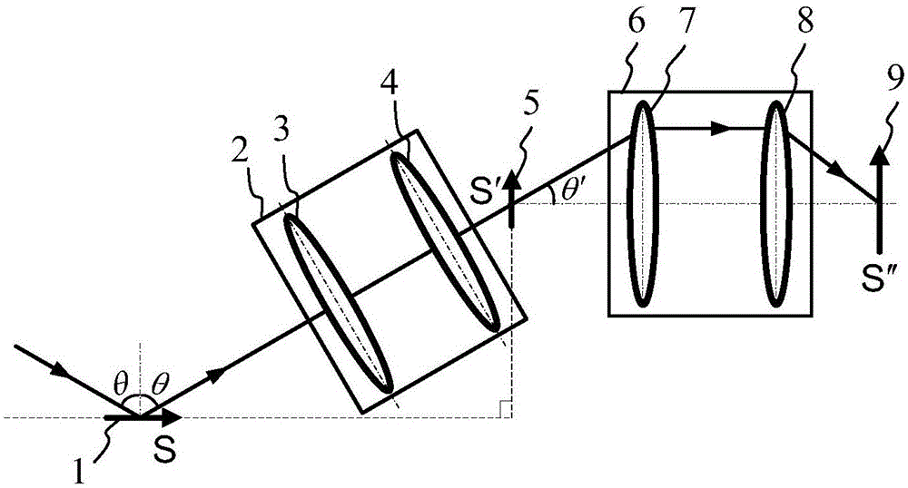
[0060] In order to make the object, technical solution and advantages of the present invention more clear, the present invention will be further described in detail below in conjunction with the accompanying drawings and embodiments. It should be understood that the specific embodiments described here are only used to explain the present invention, not to limit the present invention.

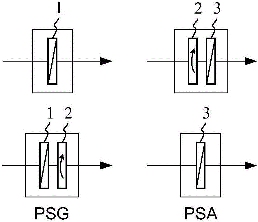
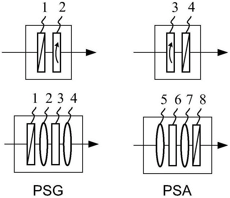
[0061] For the convenience of description, combined with the characteristics of the ellipsometry method, when describing the specific implementation, it is divided into two parts, namely: (1) the imaging spectrum ellipsometric data measurement part; (2) the measurement data analysis part. In the data measurement part, according to the different measurement parameters of the instruments, the specific implementation of the instrument for measuring the amplitude ratio angle Ψ and the phase difference angle Δ of the sample to be tested and the specific implementation of the full Muller matrix M instr...


PUM


Abstract

The invention discloses a large-area high-resolution wide-field online measurement device and a measurement method for nanostructure films. Light emitted by a light source is converted into a single-wavelength light beam through a wavelength selector, and the single-wavelength light beam is converted into an elliptic polarized beam which is then projected to a to-be-measured nanostructure film. A film reflection beam passes through an imaging unit and a polarization state analysis unit to enter an area array detector to obtain imaging spectrum ellipsometry measurement data of the to-be-measured nanostructure film. The data are matched with theoretical values and extracted to obtain parameter values of the to-be-measured nanostructure film at corresponding pixels, and the extracted parameter values form three-dimensional micrograph morphology of the to-be-measured nanostructure film. The problem that an existing device is small in focal depth value of an instrument and difficult to realize wide-field clear imaging and high-transverse-resolution measurement at the same time is solved, and large-area high-resolution accurate measurement of the nanostructure film is truly realized.

Description

technical field [0001] The invention belongs to the field of nano-manufacturing, especially the field of online process monitoring and optimization control of large-area nano-structured films in large-scale nano-manufacturing and flexible electronic manufacturing, and specifically relates to a large-area high-resolution nanostructured film (including vertical resolution and lateral resolution) resolution) wide field of view on-line measuring device and measuring method thereof. Background technique [0002] Nano-manufacturing refers to the manufacturing technology in which the characteristic size of the product is on the order of nanometers, that is, the manufacturing technology in which the characteristic size is within 100nm. In order to reduce the cost of nano-manufacturing, in recent years, in emerging industries such as flexible electronics, solar photovoltaics, and flat panel displays, roll-to-roll (roll-to-roll) or sheet-to-sheet (sheet-to-sheet) and other large-scale...

Claims


Application Information

Patent Timeline
Patent Type & Authority Applications(China)
IPC IPC(8): B82B3/00B82Y35/00
CPCB82B3/0085B82Y35/00
Inventor 陈修国陈军张传维刘世元
Owner WUHAN EOPTICS TECH CO LTD
Why Eureka
Try Eureka