Solder joint type detection method and apparatus based on image identification

A solder joint type and image recognition technology, applied in the field of automatic optical inspection, can solve the problems of troublesome plate making, low accuracy, poor stability, etc., and achieve the effect of simple and fast recognition

Inactive Publication Date: 2017-03-22
GUANGZHOU SHIYUAN ELECTRONICS CO LTD
View PDF5 Cites 42 Cited by
  • Summary
  • Abstract
  • Description
  • Claims
  • Application Information

AI Technical Summary

Problems solved by technology

However, in the actual application process, this method has problems such as troublesome plate making, low precision and poor stability.

Method used


Image

  • Solder joint type detection method and apparatus based on image identification
  • Solder joint type detection method and apparatus based on image identification
  • Solder joint type detection method and apparatus based on image identification

Examples


Embodiment 1

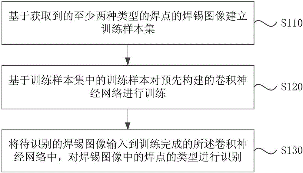
[0027] Figure 1A It is a flow chart of a solder joint type detection method based on image recognition provided by Embodiment 1 of the present invention. This embodiment is applicable to the detection of solder defects, and the method can be executed by a solder joint type detection device based on image recognition , including the following steps:

[0028] S110. Establish a training sample set based on the obtained solder images of at least two types of solder joints.

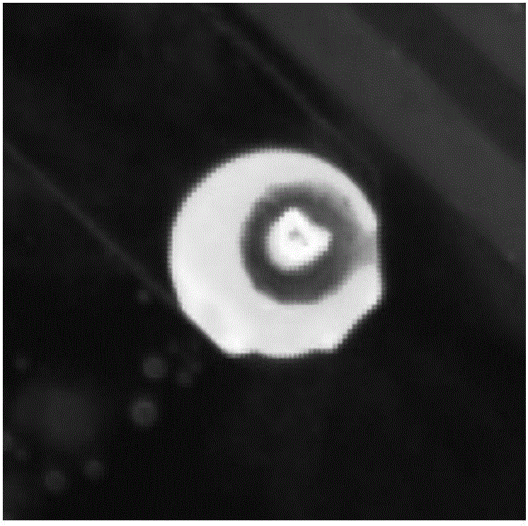
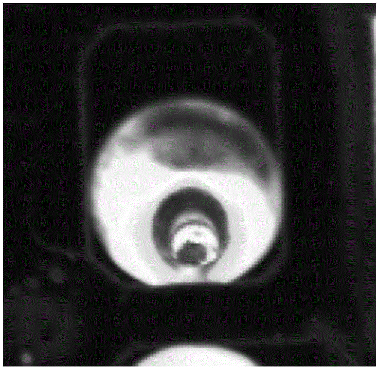
[0029] Wherein, at least two types of solder joints can include two types of solder joints, for example, the solder joints can be divided into two types: normal and abnormal; of course, more than two types of solder joints can also be included, such as Figures 1B-1E As shown, the types of solder joints can be more finely divided, such as normal ( Figure 1B ), Shaoxi ( Figure 1C ), Lianxi ( Figure 1D ) and / or multi-tin ( Figure 1E ) and other types. It can be understood that the normal solder joint t...

Embodiment 2

[0040] Figure 2A It is a flowchart of an image recognition-based solder joint type detection method provided by Embodiment 2 of the present invention. Such as Figure 2AAs shown, in this embodiment, on the basis of the above-mentioned embodiments, it is preferable to further optimize the training sample set based on the obtained solder images of at least two types of solder joints to obtain at least two types of solder joints Data expansion is performed on the original solder image; a training sample set is established based on the original solder image and the solder image after data expansion.

[0041] On this basis, it is optional that before training the pre-built convolutional neural network based on the training samples in the training sample set, it also includes: constructing a convolutional neural network comprising a parallel first subnetwork and a second subnetwork , wherein the number of layers included in the first subnetwork is greater than the number of layer...

Embodiment 3

[0068] image 3 Shown is a structural block diagram of an image recognition-based solder joint type detection device provided in Embodiment 3 of the present invention. The device can be implemented by means of hardware and / or software, and generally can be independently configured in a user terminal or server The method of this embodiment is implemented. Such as image 3 As shown, the image recognition-based solder joint type detection device specifically includes: a training sample set establishment module 310 , a convolutional neural network training module 320 and a solder joint type identification module 330 .

[0069] Wherein, the training sample set building module 310 is used to set up a training sample set based on the obtained solder images of at least two types of solder joints; the convolutional neural network training module 320 is used to pre-construct the training sample pairs based on the training sample set The convolutional neural network is trained; the sol...


PUM


Abstract

The invention discloses a solder joint type detection method and apparatus based on image identification, and relates to the technical field of automatic optical detection. The solder joint type detection method based on image identification includes the steps: based on the obtained soldering tin images of at least two types of solder joints, establishing a training sample set; based on the training samples in the training sample set, training a pre-constructed convolution neural network; and inputting soldering tin images to be identified into the pre-constructed convolution neural network which completes the training, and identifying the types of solder joints in the soldering tin images. The technical scheme of the solder joint type detection method and apparatus based on image identification can utilize the convolution neural network to identify the soldering tin images, thus solving the problem that a traditional soldering tin defect detection method has trouble in plate making and is low in precision and stability, and can simply and quickly identify the welding sport type so as to realize accurate detection of defects of soldering tin by inputting the soldering tin images into the convolution neural network which completes the training.

Description

technical field [0001] Embodiments of the present invention relate to the technical field of automatic optical inspection, and in particular to an image recognition-based solder joint type inspection and device. Background technique [0002] Automatic Optical Inspection (AOI) is a necessary part of the industrial production process. Its inspection principle is to use optical methods to obtain the surface state of the finished product, and use image processing to detect foreign objects or surface defects. The solder defect detection of solder joints on the solder surface of circuit boards is an important application in the field of circuit board defect detection. The machine takes images of the circuit boards through the camera, and the images of the circuit boards are illuminated by three-color light to obtain the three-dimensional information of the solder. Then extract the local image of the solder joints, and use image processing technology to judge whether the solder jo...

Claims


Application Information

Patent Timeline
Patent Type & Authority Applications(China)
IPC IPC(8): G06T7/00G06N3/08
CPCG06N3/08G06T7/0004G06T2207/30141
Inventor 林建民
Owner GUANGZHOU SHIYUAN ELECTRONICS CO LTD
Why Eureka
Try Eureka