Organic light-emitting display panel, electronic equipment and manufacturing method thereof

一种发光显示、有机的技术,应用在电路、电气元件、电固体器件等方向,能够解决器件效率和寿命降低、效率降低、器件寿命降低等问题,达到提高发光效率和寿命、提高发光效率、提高产率的效果

Active Publication Date: 2017-03-22
WUHAN TIANMA MICRO ELECTRONICS CO LTD +2
View PDF5 Cites 27 Cited by
  • Summary
  • Abstract
  • Description
  • Claims
  • Application Information

AI Technical Summary

Problems solved by technology

[0003] For existing organic electroluminescent devices, holes and electrons often pass through the light-emitting layer and are transported to the cathode and anode respectively. The energy of such holes and electrons cannot be used to excite the material to emit light, so that the efficiency of the device and reduced lifespan
At the same time, holes and electrons recombine to form excitons and diffuse to both sides, and some excitons will diffuse to other areas of the undoped light-emitting material, such as the hole transport layer or electron transport layer, etc., and then decay. The attenuation of such excitons cannot generate photons, which also leads to a decrease in the luminous efficiency of organic electroluminescent devices
In addition, excessive accumulation of electrons and holes in the hole transport layer and the electron transport layer will cause the material of the hole transport layer and the electron transport layer to be in an unstable charged state, and this charged substance will easily Irreversible chemical changes occur, leading to material deterioration. The most obvious change in the device is that the life of the device is reduced, and the efficiency will also be reduced.

Method used


Image

  • Organic light-emitting display panel, electronic equipment and manufacturing method thereof
  • Organic light-emitting display panel, electronic equipment and manufacturing method thereof
  • Organic light-emitting display panel, electronic equipment and manufacturing method thereof

Examples


Embodiment Construction

[0029] The present invention will be further described in detail below in conjunction with the accompanying drawings and embodiments. It should be understood that the specific embodiments described here are only used to explain the present invention, but not to limit the present invention. In addition, it should be noted that, for the convenience of description, only some structures related to the present invention are shown in the drawings but not all structures.

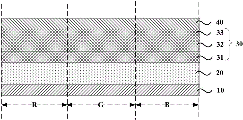
[0030] An embodiment of the present invention provides an organic light-emitting display panel, including at least a first electrode, a light-emitting layer, a first functional layer, and a second electrode that are stacked. Wherein, the first functional layer includes at least a first-type barrier layer, and the first-type barrier layer is disposed adjacent to the light-emitting layer. The first type barrier layer is doped with the first guest material; the ratio of the second type carrier mobility of the host ma...


PUM


Abstract

The invention discloses an organic light-emitting display panel, electronic equipment and a manufacturing method thereof. The organic light-emitting display panel comprises at least one first electrode, a light-emitting layer, a first functional layer and a second electrode which are arranged in a laminated manner, wherein the first functional layer at least comprises a first type of barrier layer, and the first type of barrier layer is arranged adjacent to the light-emitting layer; a first object material is doped in the first type of barrier layer; the specific value of the second type of carrier mobility of a host material of the first type of barrier layer to the second type of carrier mobility of the first object material is greater than or equal to 10; the first type is hole type, and the second type is electronic type; or the first type is electronic type, and the second type is hole type. The efficiency of the organic light-emitting display panel is improved, and the service life of the organic light-emitting display panel is prolonged.

Description

technical field [0001] Embodiments of the present invention relate to the field of display technology, and in particular to an organic light emitting display panel, an electronic device and a manufacturing method thereof. Background technique [0002] The structure of an organic electroluminescent device generally includes an anode corresponding to each pixel area, an auxiliary functional layer (such as a hole transport layer, an electron transport layer, an electron injection layer, etc.), a light-emitting layer, and a cathode. When a voltage is applied to the anode and cathode At the same time, the holes and electrons are transported to the light-emitting layer respectively, and the two recombine in the light-emitting layer to form excitons; the excitons migrate under the action of the electric field, transfer energy to the light-emitting material, and excite the electrons in the light-emitting material from The ground state transitions to the excited state, and the excite...

Claims


Application Information

Patent Timeline
Patent Type & Authority Applications(China)
IPC IPC(8): H01L27/32H01L51/50H01L51/56
CPCH10K59/00H10K50/18H10K71/00H10K85/631H10K85/6572H10K50/11H10K2101/40
Inventor 王淼滨田王湘成何为牛晶华柳晨刘营
Owner WUHAN TIANMA MICRO ELECTRONICS CO LTD
Why Eureka
Try Eureka