Resin-filled back drilling hole processing method of PCB (Printed Circuit Board)

A technology of PCB board and processing method, which is applied in the field of PCB board processing with resin plug back drilling, can solve the problems of weak signal loss, leakage of resin, incomplete exposure, etc., so as to ensure the quality of the circuit and improve the authenticity. Effect

Inactive Publication Date: 2017-03-22
SHENZHEN SUNTAK MULTILAYER PCB
View PDF3 Cites 12 Cited by
  • Summary
  • Abstract
  • Description
  • Claims
  • Application Information

AI Technical Summary

Problems solved by technology

[0006] The above-mentioned patent uses exposure and development to expose the back-drilled holes that require resin plug holes, and the resin plugs are back-drilled and smoothed, which is prone to incomplete exposure and the phenomenon that the back-drilled holes cannot be fully exposed, so it is easy to cause resin leakage. phenomenon, resulting in a weaker effect of reducing signal loss

Method used


Image

  • Resin-filled back drilling hole processing method of PCB (Printed Circuit Board)
  • Resin-filled back drilling hole processing method of PCB (Printed Circuit Board)
  • Resin-filled back drilling hole processing method of PCB (Printed Circuit Board)

Examples


Embodiment Construction

[0031] In order to fully understand the technical content of the present invention, the technical solutions of the present invention will be further introduced and illustrated below in conjunction with specific examples, but not limited thereto.

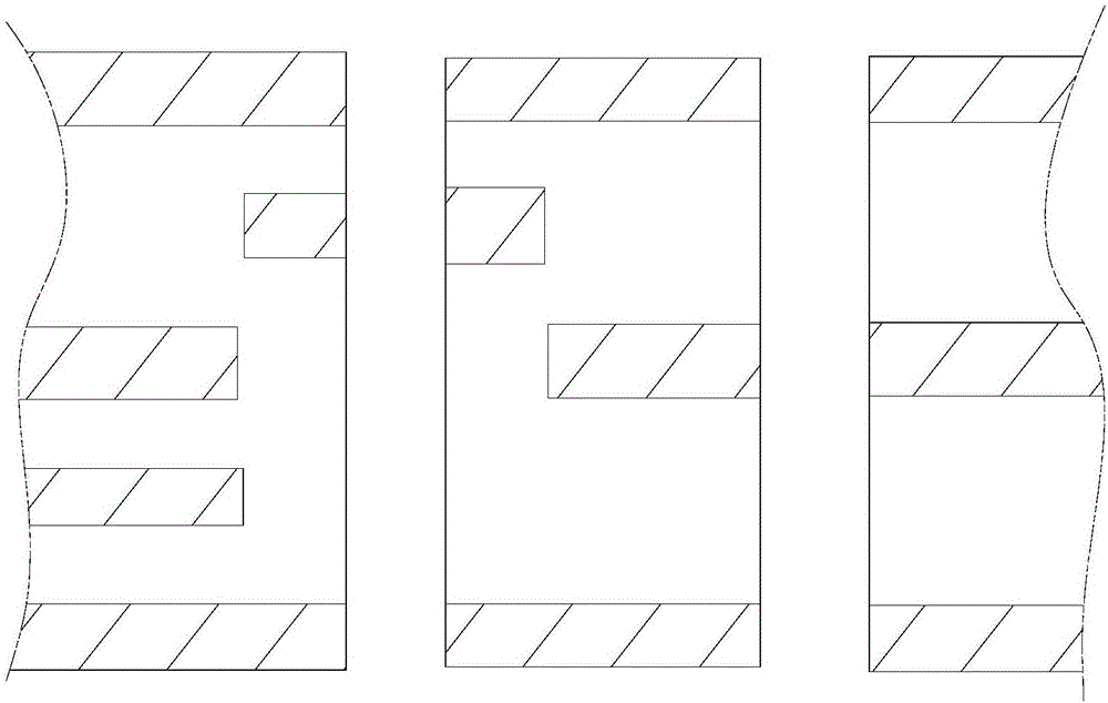
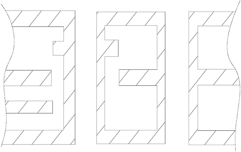
[0032] Such as Figure 1 to Figure 7 In the specific embodiment shown, the method for processing PCB boards with resin plug back drilling provided in this embodiment can be used in the process of manufacturing PCB boards to realize that the back drilling hole is NPTH and plugged with resin, and the It can ensure the quality of the line, and at the same time realize the effect that both the PTH through-hole and the NPTH back-drilled hole can be filled with resin, and can also improve the authenticity of the signal to a higher degree.

[0033] A PCB board processing method for resin plug back drilling, the method comprising:

[0034] S1. Drill through holes on the multi-layer PCB board after the previous process treatment and pressing...


PUM


Abstract

The invention relates to a resin-filled back drilling hole processing method of a PCB (Printed Circuit Board). The processing method comprises the steps of drilling through holes in a multi-layer PCB after previous procedure processing and lamination processing; plating copper to conduct the through holes, and electroplating a board surface; drilling a back drilling hole in the multi-layer PCB; filling the whole back drilling hole and the through holes which are needed to be filled with resin with the resin, grinding the board with an abrasive belt; fabricating an outer-layer pattern, covering the holes, reducing the copper, and grinding the board with the abrasive belt again; drilling a counter hole, depositing a copper plate, filling the holes with the resin for electroplating and filling; and entering a post procedure after fabricating the outer-layer pattern, electroplating the pattern, etching the outer layer, performing outer-layer AOI and performing soldering resist processing. By the processing method, the back drilling hole is an NPTH (Non Plating Through Hole) and is filled with the resin, the circuit quality is ensured, a PTH (Plating Through Hole) and the NPTH back drilling hole are both filled with the resin, and the signal reality is improved to a relatively high extent.

Description

technical field [0001] The invention relates to the technical field of circuit board manufacturing, and more specifically refers to a PCB board processing method for resin plug back drilling. Background technique [0002] The copper part of the plated through hole on the circuit board will cause the signal to fold back and resonate, resulting in reflection, scattering, delay, etc. of signal transmission, which will bring distortion to the signal. Therefore, in the PCB manufacturing process, especially in the high-speed PCB processing process, in order to prevent signal distortion or delay, it is necessary to drill the through-hole section that does not play any connection or transmission role at one end of the through-hole to reduce signal loss. That is, back drilling design. [0003] In order to increase the welding density and ensure that the position of the back-drilled hole can be soldered, it is necessary to fill the back-drilled hole with resin and fill it with electr...

Claims


Application Information

Patent Timeline
Patent Type & Authority Applications(China)
IPC IPC(8): H05K3/00H05K3/42
CPCH05K3/0044H05K3/0094H05K3/429H05K2203/0214
Inventor 翟青霞
Owner SHENZHEN SUNTAK MULTILAYER PCB
Why Eureka
Try Eureka