Semiconductor device

A semiconductor and conductive technology, which is applied in semiconductor devices, transistors, electric solid devices, etc., can solve problems such as withstand voltage drop

Active Publication Date: 2017-03-22
DENSO CORP
View PDF5 Cites 6 Cited by
  • Summary
  • Abstract
  • Description
  • Claims
  • Application Information

AI Technical Summary

Problems solved by technology

However, when no trench is formed in the diode region, electric field concentration occurs in the vicinity of the trench formed on the side of the diode region in the IGBT region, resulting in a new problem of drop in withstand voltage.

Method used


Image

  • Semiconductor device
  • Semiconductor device
  • Semiconductor device

Examples


no. 1 Embodiment approach

[0028] A first embodiment of the present invention will be described. In addition, the semiconductor device of the present embodiment is preferably used as a power switching element used in a power supply circuit such as an inverter or a DC / DC converter, for example.

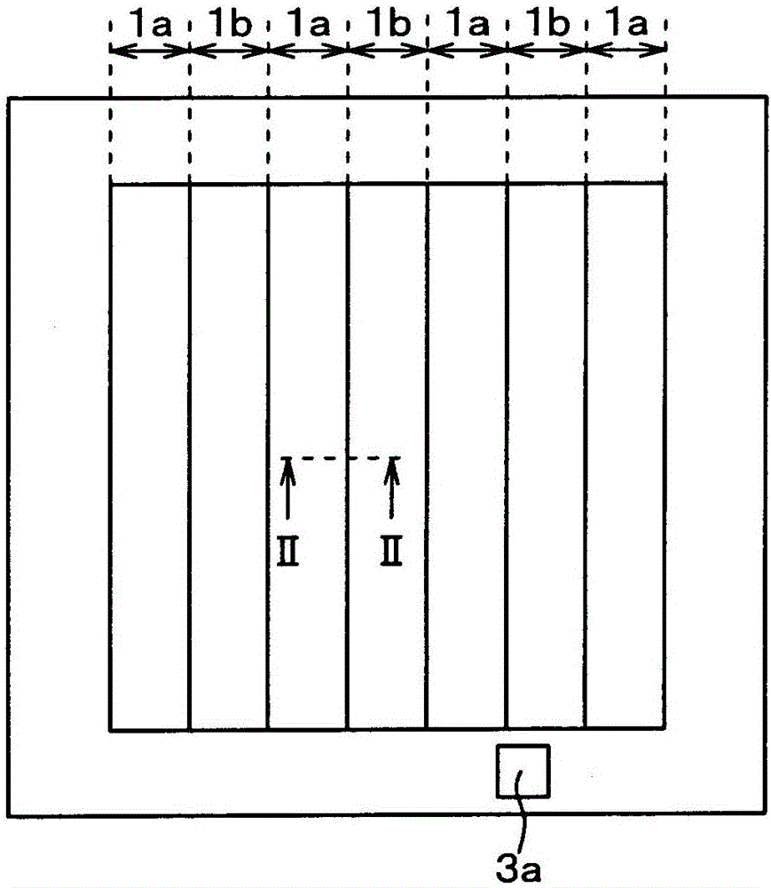
[0029] Such as figure 1 As shown, the semiconductor device has a structure in which IGBT regions 1a in which IGBT elements are formed and diode regions 1b in which diode elements are formed are alternately formed.

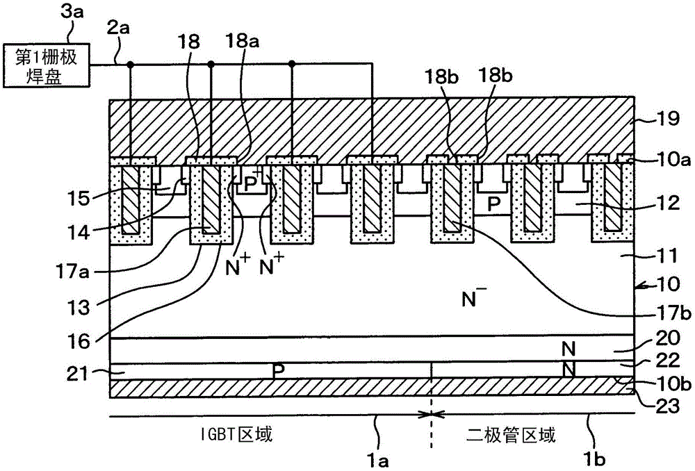
[0030] Specifically, these IGBT regions 1a and diode regions 1b are as follows figure 2 As shown, formed on the N that functions as the drift layer 11 - type common semiconductor substrate 10. In addition, in the present embodiment, the IGBT region 1a and the diode region 1b are along one direction ( figure 1 The upper and lower directions of the paper surface) are extended and formed alternately in the direction perpendicular to the extending direction.

[0031] On the drift layer 11 (on the...

no. 2 Embodiment approach

[0054] A second embodiment of the present invention will be described. In this embodiment, the second gate electrode 17 b is connected to the second gate pad as compared to the first embodiment, but the rest is the same as that of the first embodiment, so description thereof will be omitted here.

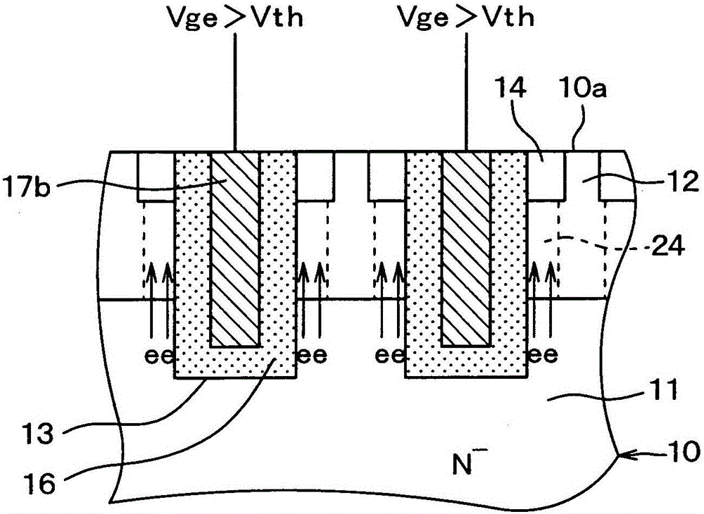
[0055] In this embodiment, if Figure 4 and Figure 5 As shown, in the semiconductor device, the second gate pad 3b is provided. Furthermore, the second gate electrode 17b is electrically connected to the second gate pad 3b via the second gate via 2b. In this embodiment, in this way, the first and second gate electrodes 17a and 17b can be controlled differently from each other.

[0056] In addition, when a semiconductor device is used, a voltage is applied to the second gate electrode 17b such that the inversion layer 24 connecting the upper electrode 19 and the drift layer 11 is not formed. For example, when a semiconductor device is used, the second gate pad 3b is connected to...


PUM


Abstract

This semiconductor device includes a drift layer (11), a base layer (12) formed on the drift layer, a collector layer (21) and a cathode layer (22) disposed opposing the base layer, a plurality of trenches (13) penetrating the base layer, gate electrodes (17a, 17b) formed in the respective trenches, an emitter region (14) formed in a surface part of the base layer in such a manner as to contact each trench, a first electrode (19) connected to the base layer and the emitter region, and a second electrode (23) connected to the collector layer and the cathode layer. The gate electrode (17b) in a diode region of the semiconductor substrate can be controlled in a different way from that of the gate electrode (17a) in an IGBT region, and a voltage is applied to the gate electrode (17b) so as not to form an inversion layer (24) in the base layer.

Description

[0001] This application claims priority based on Japanese Patent Application No. 2014-144169 filed on July 14, 2014 and Japanese Patent Application No. 2015-120461 filed on June 15, 2015, and the contents thereof are incorporated herein by reference. technical field [0002] The present invention relates to a semiconductor device having an IGBT (Insulated Gate Bipolar Transistor) region and a diode (Free Wheeling Diode) region. Background technique [0003] Conventionally, for example, as a switching element used in an inverter, a semiconductor device has been proposed in which an IGBT region in which an IGBT element is formed and a diode region in which a diode element is formed are formed on a common semiconductor substrate (for example, refer to Patent No. Literature 1). [0004] Specifically, in this semiconductor device, in the configuration N - A base layer is formed on the surface portion of the semiconductor substrate of the type drift layer, and a plurality of tren...

Claims


Application Information

Patent Timeline
Patent Type & Authority Applications(China)
IPC IPC(8): H01L29/739H01L27/04H01L29/78H01L29/861H01L29/868
CPCH01L29/78H01L27/04H01L29/407H01L29/4236H01L29/8613H01L29/0696H01L29/0834H01L29/66348H01L29/7397H01L2224/0603H01L27/0635H01L29/0804H01L29/0821H01L29/1095
Inventor 住友正清高桥茂树
Owner DENSO CORP
Why Eureka
Try Eureka