Array substrate

A technology for array substrates and glass substrates, which is applied in the field of low-temperature polysilicon array substrates, can solve problems such as unfavorable frame adhesive bonding and curing, affecting the optical taste of the panel, and uneven PI thickness, so as to enhance display performance, prevent PI liquid backflow, and improve uniformity effect

Inactive Publication Date: 2017-04-26
WUHAN CHINA STAR OPTOELECTRONICS TECH CO LTD
View PDF8 Cites 9 Cited by
  • Summary
  • Abstract
  • Description
  • Claims
  • Application Information

AI Technical Summary

Problems solved by technology

Therefore, the existing design has requirements for the width of the frame design, especially as the current design tends to be more and more narrow frame design, the PLN groove will become narrower and narrower, or even removed directly, but this is not conducive to the adhesion of the frame glue Combine and solidify
[0005] In addition, when the liquid crystal alignment liquid (PI liquid) is coated, the phenomenon of PI liquid backflow will also occur, resulting in uneven thickness of PI and affecting the optical quality of the panel.

Method used


Image

  • Array substrate
  • Array substrate
  • Array substrate

Examples


Embodiment Construction

[0027] Hereinafter, embodiments of the present invention will be described in detail with reference to the accompanying drawings. This invention may, however, be embodied in many different forms and should not be construed as limited to the specific embodiments set forth herein. Rather, the embodiments are provided to explain the principles of the invention and its practical application, thereby enabling others skilled in the art to understand the invention for various embodiments and with various modifications as are suited to particular intended uses.

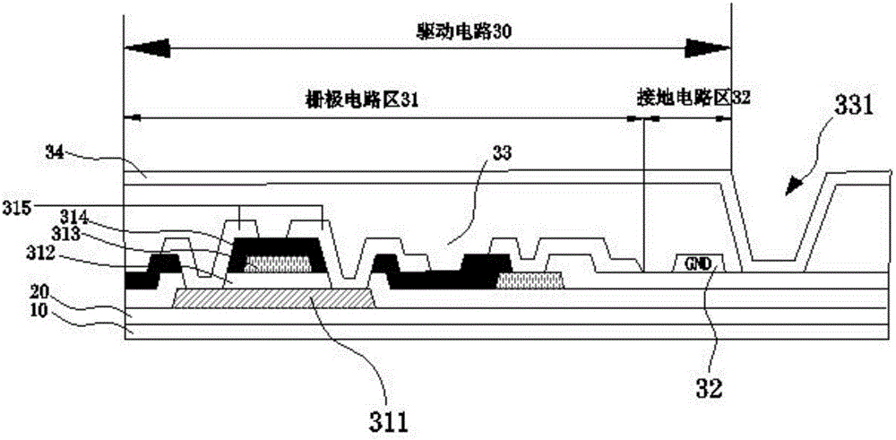
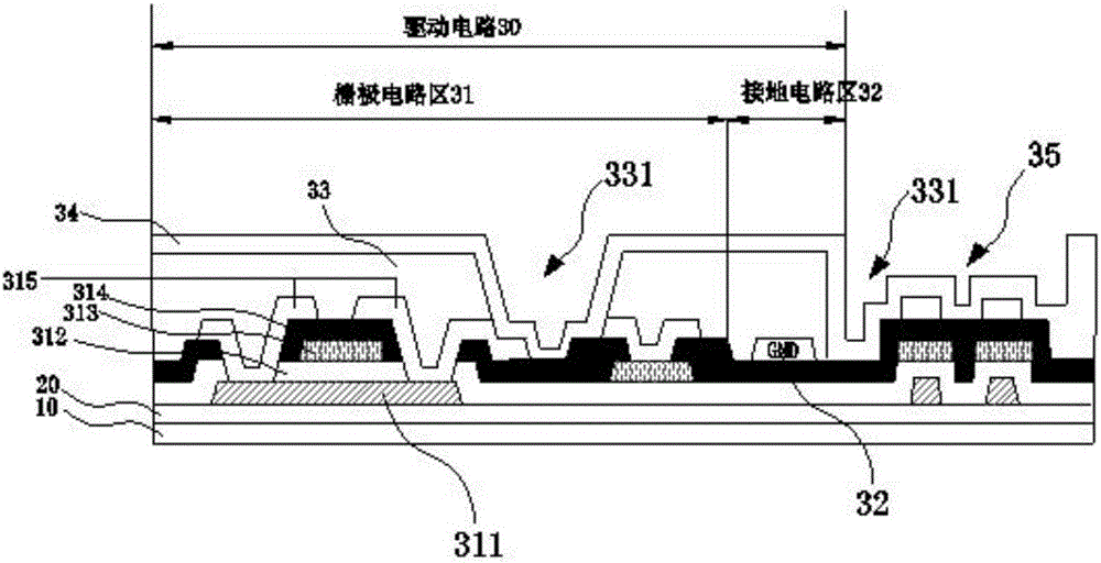
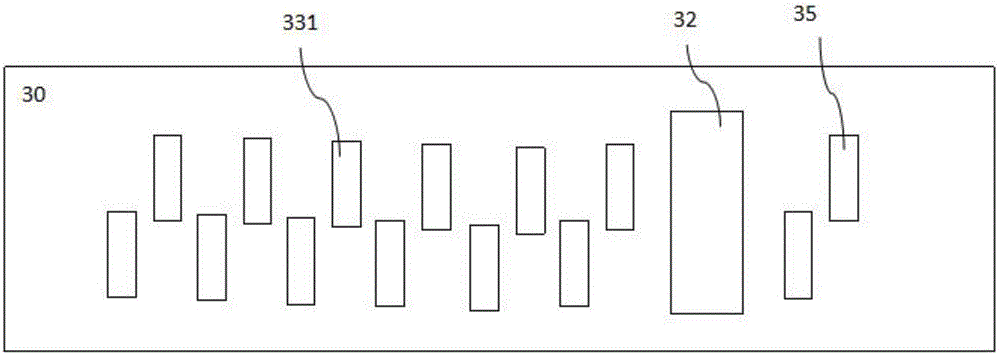
[0028] This embodiment provides an array substrate, such as figure 2 As shown, it includes from bottom to top: a glass substrate 10, a buffer layer 20, and a driving circuit 30 (GOA).

[0029] The driving circuit 30 includes a gate driving area 31 and a grounding circuit area 32 disposed around the gate driving area 31 . The surface of the driving circuit 30 is covered with a flat layer 33 (PLN) and a passivation layer 34 ...


PUM


Abstract

The invention relates to the liquid crystal display technical field, and especially discloses an array substrate. The array substrate comprises from bottom to top: a glass substrate, a buffer layer and a drive circuit. The drive circuit comprises a grid drive zone and a grounding circuit zone arranged at the periphery of the grid drive zone. A flat layer and a passivation layer sequentially cover the drive circuit from bottom to top. The flat layer, corresponding to the grid drive zone, is provided with a plurality of grooves. Contact areas between frame adhesives and the array substrate can be increased, and alignment liquid is prevented from flowing back.

Description

technical field [0001] The invention belongs to the technical field of liquid crystal display, and in particular relates to a low-temperature polysilicon array substrate. Background technique [0002] GOA technology is to integrate the gate driver on the glass substrate to scan the panel. Recently, people have increasingly studied the application of this technology on low-temperature polysilicon (LTPS) array substrates. [0003] Such as figure 1 As shown, when designing a conventional low temperature polysilicon array substrate (LTPS), the entire driving circuit 30 is covered with a thick planar layer (PLN) coating. The driving circuit 30 includes a gate driving area (GOA) 31 , and a grounding circuit area (GND) 32 is designed as a metal trace on the outermost periphery of the gate driving area 31 . In the usual design, in order to increase the adhesion of the frame glue on the frame, the PLN on both sides of the GND will be directly removed through the mask. The usual o...

Claims


Application Information

Patent Timeline
Patent Type & Authority Applications(China)
IPC IPC(8): G02F1/1333G02F1/1339G02F1/1345
CPCG02F1/1333G02F1/1339G02F1/13454
Inventor 王聪廖作敏
Owner WUHAN CHINA STAR OPTOELECTRONICS TECH CO LTD
Why Eureka
Try Eureka