Embedded touch screen and liquid crystal display apparatus
An embedded touch screen and touch screen technology, which is applied in optics, instruments, electrical digital data processing, etc., can solve the problems of low light transmittance, high production cost, and thick modules, so as to achieve enhanced effects and reduce metal reflections. Effect
- Summary
- Abstract
- Description
- Claims
- Application Information
AI Technical Summary
Problems solved by technology
Method used
Image
Examples
Embodiment 1
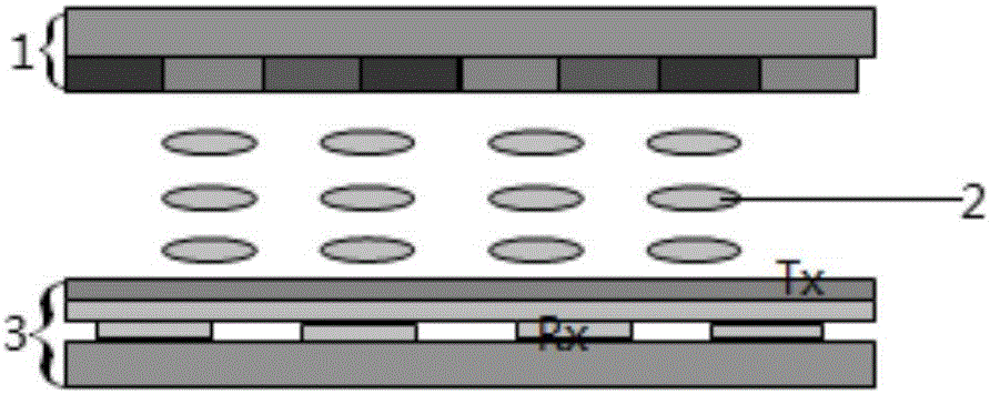
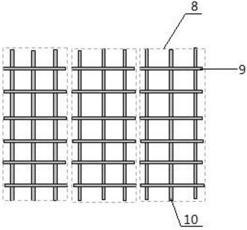
[0029] The embedded touch screen of the present invention includes an array substrate 3, and a plurality of horizontally arranged scanning lines 12 and a plurality of vertically arranged data lines 13 are formed on the surface of the array substrate 3, and the scanning lines 12 and the data lines 13 are arranged horizontally and vertically; the array The substrate 3 is sequentially prepared with a conductive light-shielding layer and an interlayer insulating layer (conductive light-shielding layer-interlayer insulating layer-scanning line metal substrate-interlayer insulating layer-data line metal layer-other layers) before preparing the scanning line metal layer, That is, the array substrate 3 is sequentially sputtered with a conductive light-shielding layer and an interlayer insulating layer under the metal layer of the scanning line; The sensing line 9 and a plurality of longitudinal sensing lines 10 distributed along the data line 13, the transverse sensing line 9 and the l...
Embodiment 2
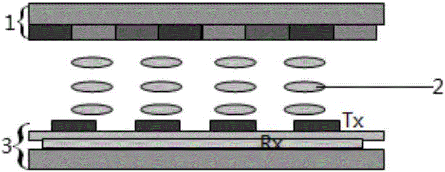
[0035] The embedded touch screen of the present invention includes an array substrate 3, and a plurality of horizontally arranged scanning lines 12 and a plurality of vertically arranged data lines 13 are formed on the surface of the array substrate 3, and the scanning lines 12 and the data lines 13 are arranged horizontally and vertically; the array The substrate 3 is sequentially prepared with a conductive light-shielding layer and an interlayer insulating layer (conductive light-shielding layer-interlayer insulating layer-scanning line metal substrate-interlayer insulating layer-data line metal layer-other layers) before preparing the scanning line metal layer, That is, the array substrate 3 is sequentially sputtered with a conductive light-shielding layer and an interlayer insulating layer under the metal layer of the scanning line; The sensing line 9 and a plurality of longitudinal sensing lines 10 distributed along the data line 13, the transverse sensing line 9 and the l...
PUM
 Abstract
Description
Claims
Application Information


