

Intelligent structure transformation system based on microelectronics technology
A technology for microelectronic process and structural transformation, which is applied in the fields of electrical digital data processing, CAD circuit design, special data processing applications, etc., and can solve problems such as device function failure.
- Summary
- Abstract
- Description
- Claims
- Application Information
AI Technical Summary
Problems solved by technology
Method used
Image

Examples
Embodiment Construction
[0044] The present invention will be further described below in conjunction with accompanying drawing.
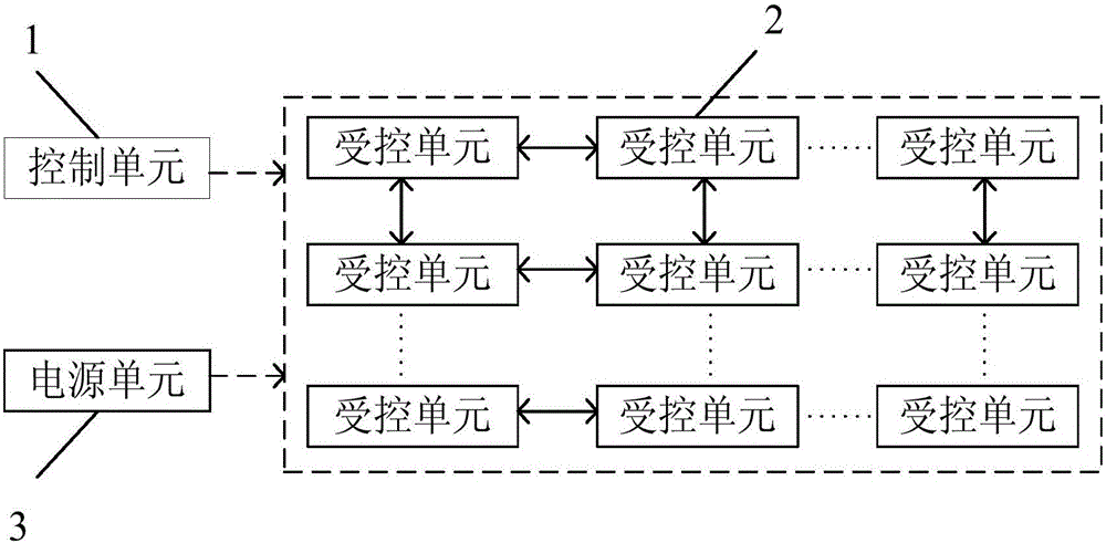
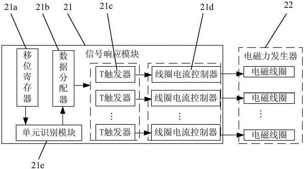
[0045] Such as figure 1 , figure 2 and Figure 10 The shown intelligent structure transformation system based on microelectronic technology includes a control unit 1, a power supply unit 3 and eight or more controlled units 2; the number of controlled units 2 is adjusted according to the actual situation. The control unit 1 is used to send a control signal and a clock signal, and the control signal includes a unit identification code and an electromagnetic coil selection code. The power supply unit 3 is connected to each controlled unit 2 to supply power to each controlled unit 2 . Each controlled unit 2 has an independent unit identification code, and each controlled unit 2 is at least in contact with another controlled unit 2 . The controlled unit 2 includes a cube-shaped housing, and an electromagnetic force generator 22 and a signal response module 21 arranged in t...
PUM
 Abstract
Description
Claims
Application Information