Apparatus and method for improving threshold voltage distribution of nonvolatile storage apparatus
A non-volatile storage and voltage distribution technology, applied in static memory, read-only memory, information storage, etc., can solve the problems of difficult control of programming time and insufficient programming efficiency of programming time
Inactive Publication Date: 2017-04-26
MACRONIX INT CO LTD
5 Cites 0 Cited by
AI-Extracted Technical Summary
Problems solved by technology
In this regard, challenges presented by large diameters can be, for example, programming inefficiencies in terms of programming time
I...
Abstract
The invention provides a method for controlling voltage threshold value distribution corresponding to a nonvolatile storage apparatus and a related apparatus, and a memory cell of the nonvolatile storage apparatus executes a function. In one embodiment, a method is provided. The method comprises provision of the nonvolatile storage apparatus. The apparatus comprises one or several strings, each string comprises several memory cells, and the memory cells comprise a first memory cell and a second memory cell. The method also comprises the following steps: application of a first functional voltage to the first memory cell and application of a second functional voltage to the second memory cell, in order to execute a function of the nonvolatile storage apparatus. The first functional voltage and the second functional voltage are different.
Application Domain
Read-only memories
Technology Topic
Storage cellVoltage +2
Image
Examples
- Experimental program(1)
Example Embodiment
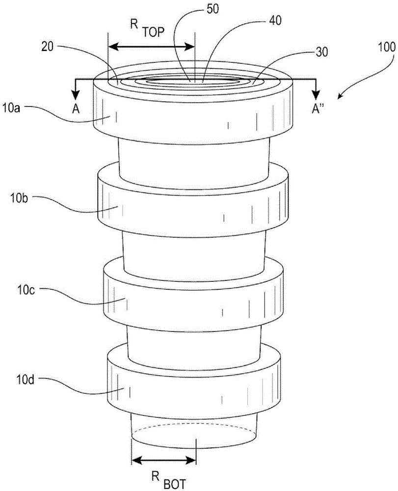
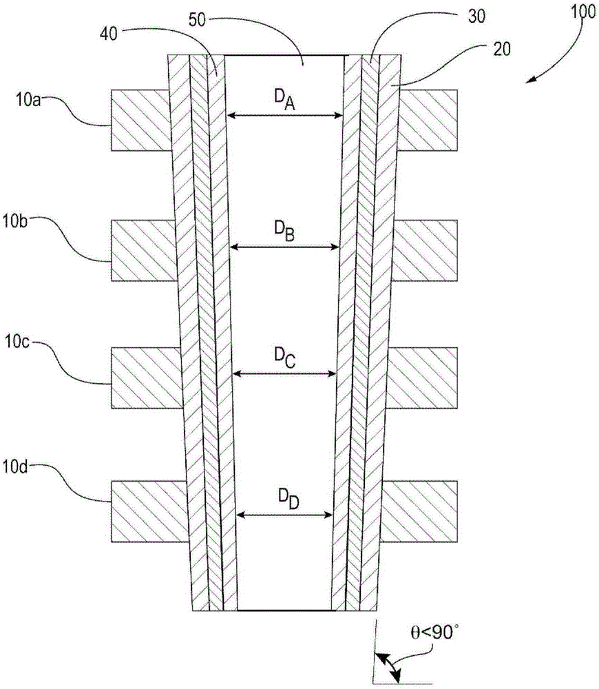
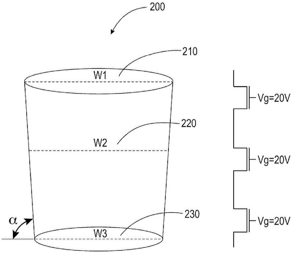
[0036] Herein, some embodiments of the present invention are described in detail with reference to the accompanying drawings, but not all embodiments are shown in the drawings. Indeed, these inventions can use many different variations and are not limited to the examples herein. Rather, the present invention provides these embodiments to meet the statutory requirements of the application. The same reference symbols are used in the drawings to designate the same or similar elements.
[0037] Although specific terms are employed herein, they are used in a generic and descriptive sense only and not for purposes of limitation. Unless defined otherwise, all terms used herein including technical and scientific terms have the same meaning as commonly understood by one of ordinary skill in the art of the invention. It will be further understood that terms such as those defined in commonly used dictionaries should be interpreted to have meanings as commonly understood by those of ordinary skill in the art. It will be further understood that terms such as those defined in commonly used dictionaries should be interpreted to have meanings consistent with the relevant art and the context of the present invention. Unless expressly so defined in this disclosure, these generally used terms are not to be interpreted in an idealized or overly formal sense.
[0038] The "gate structure" mentioned herein refers to elements in a semiconductor device, such as a memory device. Non-limiting examples of storage devices include flash memory devices (eg, NAND flash memory devices). Erasable Programmable Read-Only Memory (EPROM) and Electrically Erasable Programmable Read-Only Memory (EEPROM) are non-limiting examples of flash memory devices. The gate structure of the present invention may be a collection of gate structures operable in a memory device, or a subset of one or more elements of the gate structure.
[0039] A "non-volatile memory device" as used herein refers to a semiconductor device that can store information even after power is removed. Non-volatile memory devices include, but are not limited to, Mask Read-Only Memory, Programmable Read-Only Memory, Erasable Programmable ROM, Electrically Erasable Programmable Read-Only Memory (Electrically Erasable Programmable Read-Only Memory), and flash memory, such as NAND and NOR flash memory.
[0040] The "substrate" mentioned herein may include any underlying material on which devices, circuits, epitaxial layers or semiconductors may be formed. In general, a substrate may be used to define layers underlying a semiconductor device, or to form a base layer of a semiconductor device. The substrate may include one or any combination of silicon, doped silicon, germanium, silicon germanium, semiconductor compound, or other semiconductor materials.
[0041] The gate structures (eg, nonvolatile memory devices) and methods of the present invention improve the programming threshold voltage distribution of nonvolatile memory devices for random access, such as 3D NAND flash memory. For this reason, the programming speed of the nonvolatile memory device will increase based on the non-uniform programming voltage.
[0042] The present invention is concerned with a variety of functions including programming (eg PGM), erasing (eg ERS), reading (eg READ) or any other function that applies a voltage to multiple memory cells on the same string. The present invention can be implemented in different types of devices and/or storage units, including 3D NAND flash memory, other non-volatile storage devices (such as 3D NOR, 3D ROM, 2D NAND or 2D NOR), MOS storage in regular configuration unit or any other device for voltage control in a regular configuration. For illustration purposes, this article provides an example of programming 3D NAND flash memory. Based on the disclosure provided herein, those skilled in the art can understand how to apply the present invention to other functions and other types of devices.
[0043] Figure 1A and Figure 1B A portion of a non-volatile memory device such as 3D NAND flash memory is shown. Figure 1B for along Figure 1AThe line A-A" is a tangent line, and the cross-sectional drawing is drawn. The portion of the depicted nonvolatile memory device includes a vertical string 100 that includes a plurality of memory cells. The depicted string 100 includes four memory cells However, in different embodiments, the string 100 may include more than four or less than four memory cells depending on the application. In general, the string 100 usually includes word lines 10a, 10b, 10c, and 10d (for example, Corresponding to the word line of each memory cell) wraps around the cylindrical part. It should be noted that although the string 100 is generally cylindrical, it is actually slightly conical. The process of etching the multiple layers of the string makes the string slightly deviates from the standard. Therefore, the exterior angle θ is less than 90°. This makes the radius R at the top of the string TOP will be smaller than the radius R at the bottom of the string BOT Come big. Therefore, the channel width of each memory cell in the string 100 is different from that of adjacent memory cells (for example, D AD BD CD D ).
[0044] In general, the NAND string 100 includes a tunneling layer 40 surrounding the channel region 50 , a trapping layer 30 and a barrier or dielectric layer 20 . In various embodiments, the tunneling layer 40 may be composed of oxide and have a thickness of about 5 nm. In some embodiments. The blocking or dielectric layer 20 may be composed of oxide and have a thickness of about 7 nm. Channel region 50 may comprise polysilicon material or other suitable materials. Word lines (eg, 10a, 10b, 10c, and 10d) surround barrier or dielectric layer 20 such that there is one word line per memory cell. The word lines (eg, 10a, 10b, 10c, and 10d) may be composed of polysilicon material, metal, or other suitable materials.
[0045] Figure 2A and Figure 2B Normal operation of a NAND string 200 with three memory cells 210 , 220 and 230 is shown. In this example, the channel diameter or width W1 of the memory cell 210 is 100 nm, the channel diameter or width W2 of the memory cell 220 is 90 nm, and the channel diameter or width W3 of the memory cell 230 is 80 nm. During the execution of the programming function, the uniform voltage V g =20V is applied to each memory cell through its own word line. When the programming function is performed, the programming valve voltage distribution is widened due to the speed difference between the memory cells due to the difference in the channel diameter or width of the memory cells. Therefore, according to this example, when a uniform voltage of 20V is applied, because of the difference in width of the three memory cells 210, 220, 230, it should be noted that although the memory cell string 200 is generally cylindrical, it is actually slightly conical. The process of etching multiple layers of the string causes the string to deviate slightly from standard. Therefore, the external angle α is smaller than 90°. The programming voltage results in a wide programming valve voltage variation over time5. As shown in the figure, when the channel width of a memory cell is larger, the programming time of the memory cell is longer. On the contrary, when the channel width of a memory cell is smaller, the programming time of the memory cell is shorter. As shown in Figure 2B, at time 1x 10 -5 Seconds, the programming valve voltage variation 5 of the three memory cells is about 1-1.5V. Due to the difference in channel width among the three memory cells, the variation among the three memory cells is about 20% of the valve voltage of each memory cell.
[0046] The present invention proposes a method to reduce the variation of the valve voltage of the memory cells along the string, thereby making the valve voltage distribution tighter. Figure 3A and Figure 3B An example of this method is shown. Figure 3A The string 200 is shown to include examples of memory cells 210, 220, and 230, wherein, in this example, the channel diameter or width of the memory cell 210 is 100 nm, the channel diameter or width of the memory cell 220 is 90 nm, and the channel diameter of the memory cell 230 is 100 nm. Or a width of 80nm. A non-uniform voltage is applied instead of a uniform voltage of 20V to each memory cell via the corresponding word line. Therefore, the word line of the memory cell 210 applies the programming voltage V to the memory cell 210 g =20V, the word line of the memory cell 220 applies the programming voltage V to the memory cell 220 g =19.5V, and the word line of memory cell 230 applies programming voltage V to memory cell 230 g =19V. Therefore, a program voltage applied to a memory cell having a smaller channel diameter or width is smaller than a program voltage applied to a memory cell having a larger channel diameter or width. Figure 3B Plotted are the valve voltage variations of the three memory cells as a function of time when operated with non-uniform programming voltages. In particular, at times 1x 10 -5 Seconds, the valve voltage variation 6 of the three memory cells is the smallest. For this reason, applying a non-uniform voltage can reduce the variation of the programming valve voltage among the memory cells and reduce the programming time.
[0047] In various embodiments, the programming voltage applied to each memory cell in a string via the corresponding word line can be used to minimize the variation in the valve voltage of the memory cells in the string. For example, the programming voltage of each memory cell in the string, V g , can be different. In other embodiments, the string can be divided into two segments or groups, where a first programming voltage is applied to memory cells whose channel diameter or width is equal to or greater than a threshold, and a second programming voltage is applied to the channel Storage cells with a diameter or width smaller than this threshold. In this case, the first programming voltage may be greater than the second programming voltage. In various embodiments, multiple threshold widths can be used to divide the string into sectors or groups, where the memory cells in each sector or group are provided with a specific programming voltage.
[0048] In various embodiments, the difference in programming voltages applied to two memory cells may be based on the difference in channel width between the two memory cells. In other embodiments, the programming voltage difference between two adjacent memory cells may be predetermined rather than based on the channel width difference between the two adjacent memory cells. For example, in some embodiments, the programming voltage difference between any two pairs of adjacent memory cells is the same. This refers to a regular programming voltage distribution. Therefore, in the above example, the difference between the programming voltages applied to the memory cells 210 , 220 is the same as the difference between the programming voltages applied to the memory cells 220 , 230 . In other embodiments, the programming voltages between the first pair of adjacent memory cells and the second pair of adjacent memory cells may be different. This refers to an irregular programming voltage distribution. For example, the difference between the programming voltages applied to the memory cells 210 , 220 is different from the difference between the programming voltages applied to the memory cells 220 , 230 .
[0049] One of ordinary skill in the art will appreciate that the programming voltage profile applied to a particular string of memory cells can be used to minimize the variation in the valve voltage of the string of memory cells, taking into account other operating constraints. For example, the same programming voltage distribution can be applied to each string comprising semiconductor devices. In another example, a device may be limited to provide k (k is a positive integer) different programming voltages along each string, but a string may include n (n is a positive integer) different memory cells.
[0050] Figure 4A and Figure 4B Draw two examples of programming voltage distributions applied to n memory cells in a string, where ΔV g is a programmed voltage change. For example, in Figure 3A and Figure 3B In the example shown, the difference between the programming voltages applied to memory cells 210 and 220 and the difference ΔV between the programming voltages applied to memory cells 220 and 230 g All are 0.5V. As noted above, in various embodiments, the programming voltage distribution may be regular (e.g., the ΔV between any two adjacent memory cells or groups g can be constant), or the programming voltage distribution can be irregular (for example, ΔV between adjacent memory cells or groups g can be different).
[0051] Figure 5 An example string including N (N is a positive integer) memory cells is shown. Each memory cell corresponds to a word line, as shown labeled WL1, WL2, WL3, . . . , WLN. The N storage units are divided into n (n is a positive integer less than or equal to N) groups. In some embodiments, the plurality of memory cells in each group are identical. In other embodiments, some groups may include different numbers of memory cells among them. However, each group includes at least one memory cell. Each group is applied with a specific programming voltage. For example, group 1 may include 5 memory cells with the largest channel width among all memory cells along the string, and group 2 may include 4 memory cells with the smallest channel width among all memory cells along the string. The first programming voltage can be applied to the memory cells of the group 1 through the word lines corresponding to the memory cells of the group 1, and the second programming voltage can be applied to the memory cells of the group 2 through the word lines corresponding to the memory cells of the group 2. 2 on these storage units. In this example, the first programming voltage is greater than the second programming voltage.
[0052] Figure 5 The right-hand plot of FIG. 1 shows the effect of the group number of n groups of memory cells along the string on the valve voltage distribution, where each group is applied with a specific programming voltage, and each group is applied with a different specific programming voltage. For example, all the memory cells in the group 1 are applied with the first programming voltage, and all the memory cells in the group 2 are applied with the second programming voltage, and the first programming voltage and the second programming voltage are not equal. When the number of n groups of memory cells along a string is small, dividing the memory cells along the string into n+1 groups can significantly reduce the valve voltage compared to dividing the memory cells along the string into n groups The width of the distribution. However, after point P, increasing the group number only moderately reduces the width of the valve voltage distribution. Thus, in one embodiment, the number of groups used will coincide with point P such that the valve voltage distribution is reduced and the effect of applying non-uniform programming voltages on other performance characteristics of the memory device is minimized.
[0053] Image 6 A flowchart of a process 400 for controlling a programming valve voltage distribution corresponding to a non-volatile memory device according to an embodiment of the present invention is shown. The process 400 begins with step 410, providing a storage device (such as a 3D NAND flash storage device). A memory device may include one or more strings, each string including a plurality of memory cells, such as Figure 1A and Figure 1B shown. Each memory cell corresponds to a portion of the channel area of the string. This portion of the channel area has a specific channel width associated therewith. In step 420, the number of groups used in each string is determined. For example, in one embodiment, something similar to Figure 5 The analysis shown was used to decide the optimal number of groups for each group. In other embodiments, operating constraints or other constraints may be used to determine the number of groups in each string. At step 430, the memory cells in the string are allocated into the groups. For example, the first five memory cells in a string can be assigned to bank 1, the next five memory cells along the string can be assigned to bank 2, and so on.
[0054] In step 440, a programming voltage distribution to be applied to each group is determined. In various embodiments, this step may include analyzing the channel widths of the memory cells in the group (e.g., comparing the average channel width of the memory cells in group 1 to the average channel width of the memory cells in group 2 to determine the programming between group 1 and group 2 Voltage difference). In various embodiments, the memory cells of the string are not grouped and the programming voltage for each memory cell is determined. In some embodiments, the distribution of programming voltages may be determined based on operating constraints and/or other constraints.
[0055]At step 450, programming functions are implemented. For example, a programming voltage may be applied to each memory cell via a corresponding word line to program the memory cells of a string. The program voltage applied to each memory cell may be based on a predetermined distribution of program voltages. In effect, the programming voltage profile is applied to the memory cells along the string such that the programming voltage applied to a memory cell on the string is different from the programming voltage applied to a second memory cell on the string, thereby reducing the programming voltage along the string. The valve voltage variation of the memory cells of the string. Those of ordinary skill in the technical field of the present invention should understand that, as mentioned above, the present method can be used for various functions, including programming, erasing, reading, and other functions of applying voltage to the memory cells of the same string. Furthermore, it should be understood that the present invention is applicable to various types of semiconductor devices including non-volatile memory devices such as 3D NOR, 3D ROM, 2D NAND, 3D NAND, 2D NOR, MOS memory cells in regular configuration, Or any other device for voltage control in a regular configuration.
[0056] In different embodiments, steps 420-440 may be performed once for a device. Next, at each time a function (eg, PGM, ERS, Read, etc.) is performed, a predetermined voltage profile is applied as described herein to control the variation in the valve voltage of the memory cells along each string. For example, a predetermined voltage distribution can be accessed and applied instead of performing steps 420-440 to determine the voltage distribution each time a function is to be performed.
[0057] One aspect of the present invention is to provide a non-volatile storage device programmed according to a method of the present invention.
[0058] Various modifications and other embodiments of the inventions presented herein will come to mind to one of ordinary skill in the art having the benefit of the teachings presented in the foregoing descriptions and the associated drawings. Therefore, it is to be understood that the inventions are not to be limited to the specific embodiments disclosed and that modifications and other embodiments are to be included within the scope of the following claims. Furthermore, while the above description and associated drawings describe embodiments in the context of certain illustrative combinations of elements and/or functions, it should be understood that different combinations of elements and/or functions may be made without departing from the claims below. provided by alternative embodiments under the category of . Here, for example, combinations of elements and/or functions other than those detailed above are also contemplated as may be presented in some of the following claims. Although specific terms are employed herein, they are used in a generic and descriptive sense only and not for purposes of limitation.
[0059] In summary, although the present invention has been disclosed as above with preferred embodiments, it is not intended to limit the present invention. Those skilled in the art to which the present invention belongs may make various changes and modifications without departing from the spirit and scope of the present invention. Therefore, the protection scope of the present invention should be determined by what is defined by the claims.
PUM


Description & Claims & Application Information
We can also present the details of the Description, Claims and Application information to help users get a comprehensive understanding of the technical details of the patent, such as background art, summary of invention, brief description of drawings, description of embodiments, and other original content. On the other hand, users can also determine the specific scope of protection of the technology through the list of claims; as well as understand the changes in the life cycle of the technology with the presentation of the patent timeline. Login to view more.