Liquid crystal display device

A technology of liquid crystal display devices and liquid crystal display panels, which is applied in the direction of instruments, nonlinear optics, optics, etc., can solve the problems of waste of process time, product quality degradation, high precision and stability requirements, etc., to improve heat dissipation and product cost Low, good display effect

Active Publication Date: 2019-11-08
TCL CHINA STAR OPTOELECTRONICS TECH CO LTD
View PDF5 Cites 0 Cited by
  • Summary
  • Abstract
  • Description
  • Claims
  • Application Information

AI Technical Summary

Problems solved by technology

The advantage of this method is that the process is simple and mature, and it is widely used in the industry, but there are many problems at the same time: first, the gold material coated with resin balls in the conductive gold glue is expensive, and for large-scale production, it will increase the efficiency of liquid crystal display devices. cost; at the same time, as mentioned above, this method of conducting the Array substrate and the CF substrate requires two processes of frame glue coating and conductive gold glue titration. Usually, the process of titrating the conductive gold glue will take up a piece of panel glue coating. It takes more than half of the process time to fabricate, which greatly wastes the process time, and the method of titrating the conductive gold glue has high requirements on the accuracy and stability of the machine. A slight deviation will cause the individual conductive gold glue to be too large after lamination. , leading to problems such as cutting and scrapping, abnormal liquid crystal alignment, and low yield, which increase production costs and reduce product quality; again, based on different design driving frequencies, the metal wires around the liquid crystal display device are subjected to high-frequency current shocks , it is very easy to heat up the periphery of the liquid crystal display device, and the long-term heat accumulation will cause the aging of the glue around the liquid crystal display device, resulting in poor reliability and burns on the upper and lower polarizers.

Method used


Image

  • Liquid crystal display device
  • Liquid crystal display device
  • Liquid crystal display device

Examples


Embodiment Construction

[0030] In order to further illustrate the technical means adopted by the present invention and its effects, the following describes in detail in conjunction with preferred embodiments of the present invention and accompanying drawings.

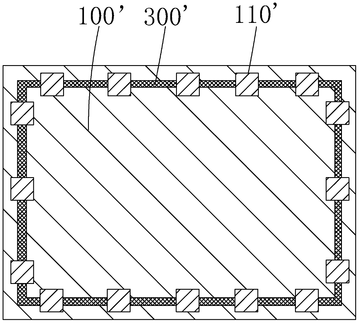
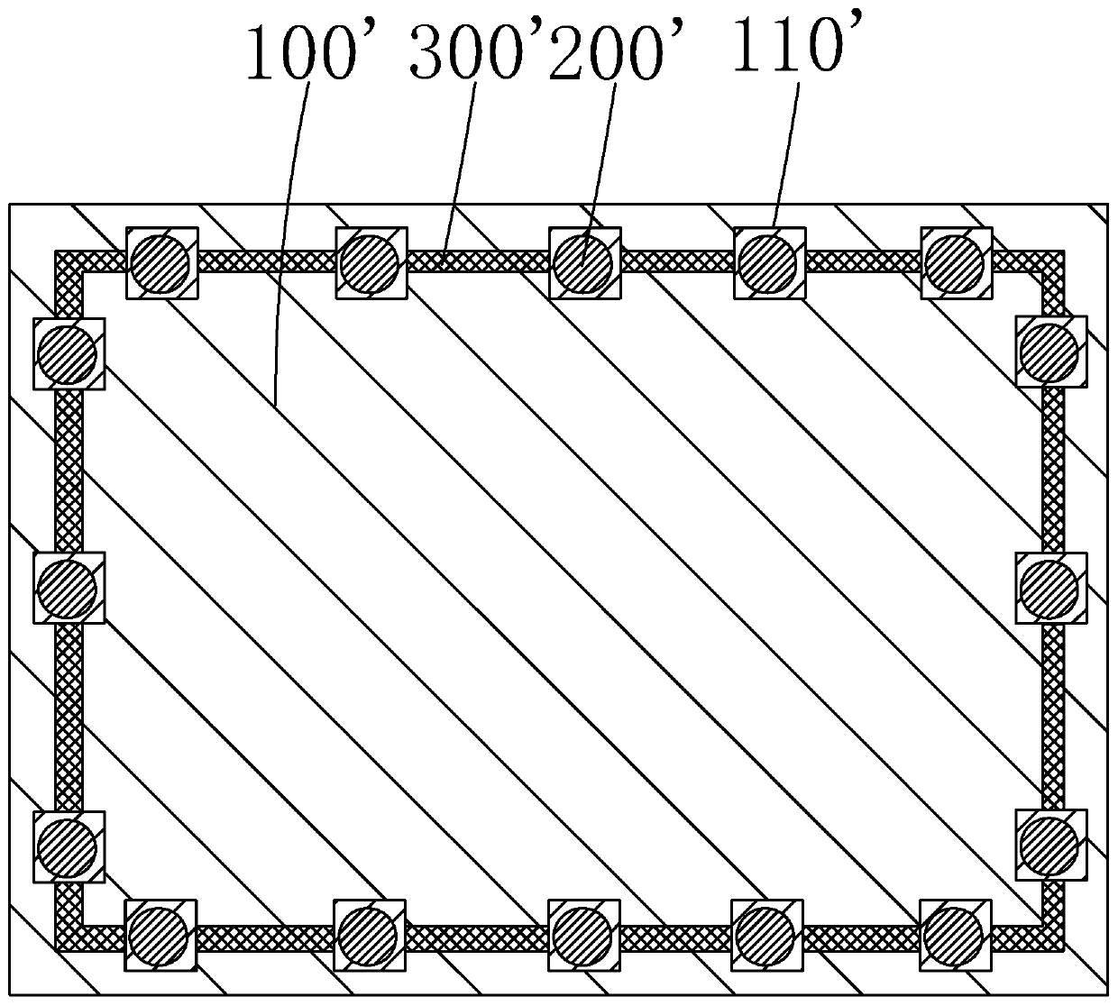
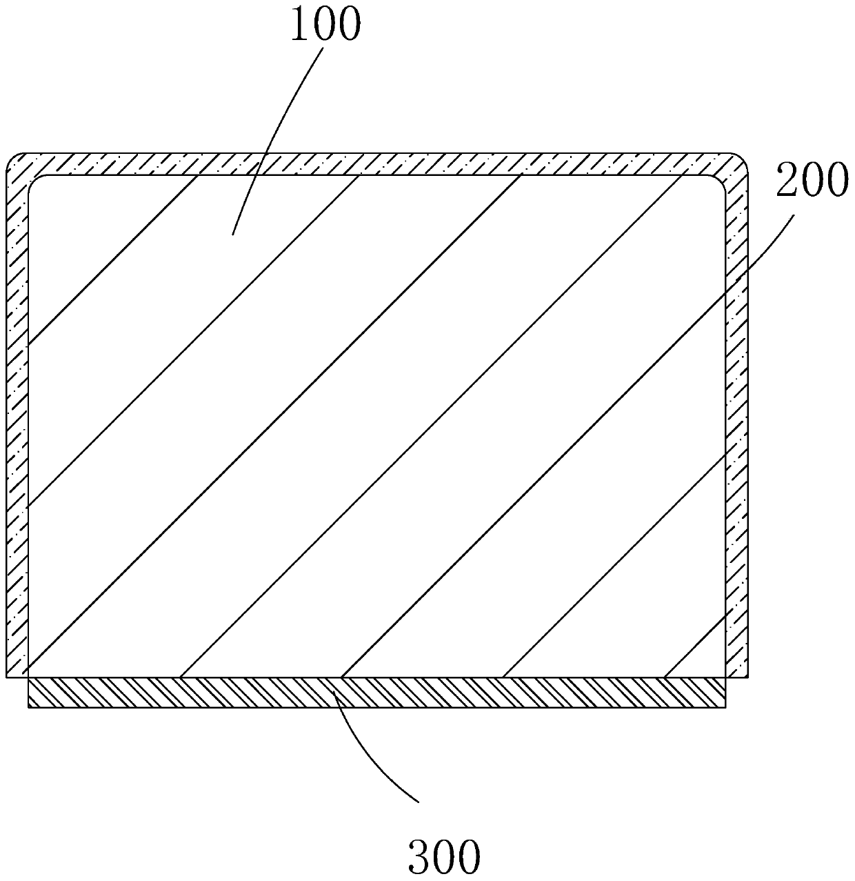
[0031] see image 3 , the present invention provides a liquid crystal display device, comprising a liquid crystal display panel 100 and a conductive light-shielding layer 200 coated on the side of the liquid crystal display panel 100 .

[0032] Specifically, the shape of the liquid crystal display panel 100 is rectangular, including four sides, and the liquid crystal display device further includes a circuit board 300 connected to one side of the liquid crystal display panel 100, and the liquid crystal display panel 100 Among the four sides, except the side connected to the circuit board 300 , the other three sides are coated with the conductive light-shielding layer 200 .

[0033] see Figure 4 or Figure 5 , the liquid crystal display pan...


PUM


Abstract

The invention provides a liquid crystal display device. A first epitaxial electrode layer which is used for connecting a conduction point and extends towards the outer side of an array substrate is arranged at the edge of the array substrate, a second epitaxial electrode layer which extends towards the outer side of a color film substrate is arranged at the edge of the color film substrate, at the same time a conduction light-shielding layer which is coated with graphene and light-shielding materials is arranged at the broadside of a liquid crystal display panel, wherein the conduction light-shielding layer is capable of shielding the light leakage around the liquid crystal display device, and is capable of simultaneously connecting the first epitaxial electrode layer and the second epitaxial electrode layer so that breakover is achieved between the array substrate and the color film substrate. Compared with the prior art, conducive gold gum does not need to be produced, the producing time is short, and the product cost is short; meanwhile, due to the fact that graphene has high thermal conductivity efficiency and high electricity conductivity rate, the heat dissipation capability around the liquid crystal display device can be promoted, and the liquid crystal display device is uniform in overall electricity, good in display effect, and has an anti-static function.

Description

technical field [0001] The invention relates to the technical field of liquid crystal display, in particular to a liquid crystal display device. Background technique [0002] As a leader in flat panel displays, thin film transistor liquid crystal displays (Thin Film Transistor Liquid Crystal Display, TFT-LCD) have gradually occupied the display due to its low power consumption, excellent picture quality and high production yield. dominance in the field. Most of the liquid crystal displays currently on the market are backlight liquid crystal display devices, which include a liquid crystal display panel and a backlight module. Generally, a liquid crystal display panel is composed of a color filter (Color Filter, CF) substrate, an array (Array) substrate, a liquid crystal sandwiched between the color filter substrate and the array substrate, and a sealant. The liquid crystal display controls the orientation of the liquid crystal molecules through the electric field, changes t...

Claims


Application Information

Patent Timeline
Patent Type & Authority Patents(China)
IPC IPC(8): G02F1/1362G02F1/1333
CPCG02F1/133385G02F1/136204G02F1/136209
Inventor 马超
Owner TCL CHINA STAR OPTOELECTRONICS TECH CO LTD
Why Eureka
Try Eureka