A kind of nand Flash bad block management method, device and memory

A management method and memory technology, applied in the NandFlash bad block management method, devices and memory fields, can solve the problems of occupying RAM resources, incorrect, FPGA programs cannot run, etc., and achieve the effect of saving occupied space and saving internal resources

Active Publication Date: 2020-04-21
BEIJING LUSTER LIGHTTECH
View PDF4 Cites 0 Cited by
  • Summary
  • Abstract
  • Description
  • Claims
  • Application Information

AI Technical Summary

Problems solved by technology

[0004] However, RAM requires at least 12bit bytes when storing block addresses, and the Nand Flash module usually contains a large number of blocks (such as 4096 blocks), so the RAM inside the FPGA must occupy at least 12bit wide and 4096 deep bytes. Therefore, the above bad block management method occupies a large amount of FPGA internal RAM resources, especially when the internal resources of the PFGA are tight, it will cause the FPGA program to fail or run incorrectly.

Method used


Image

  • A kind of nand Flash bad block management method, device and memory
  • A kind of nand Flash bad block management method, device and memory
  • A kind of nand Flash bad block management method, device and memory

Examples


Embodiment Construction

[0061] Reference will now be made in detail to the exemplary embodiments, examples of which are illustrated in the accompanying drawings. When the following description refers to the accompanying drawings, the same numerals in different drawings refer to the same or similar elements unless otherwise indicated. The implementations described in the following exemplary examples do not represent all implementations consistent with the present invention. Rather, they are merely examples of apparatuses and methods consistent with aspects of the invention as recited in the appended claims.

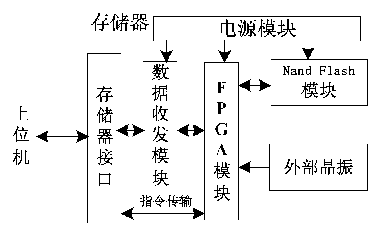
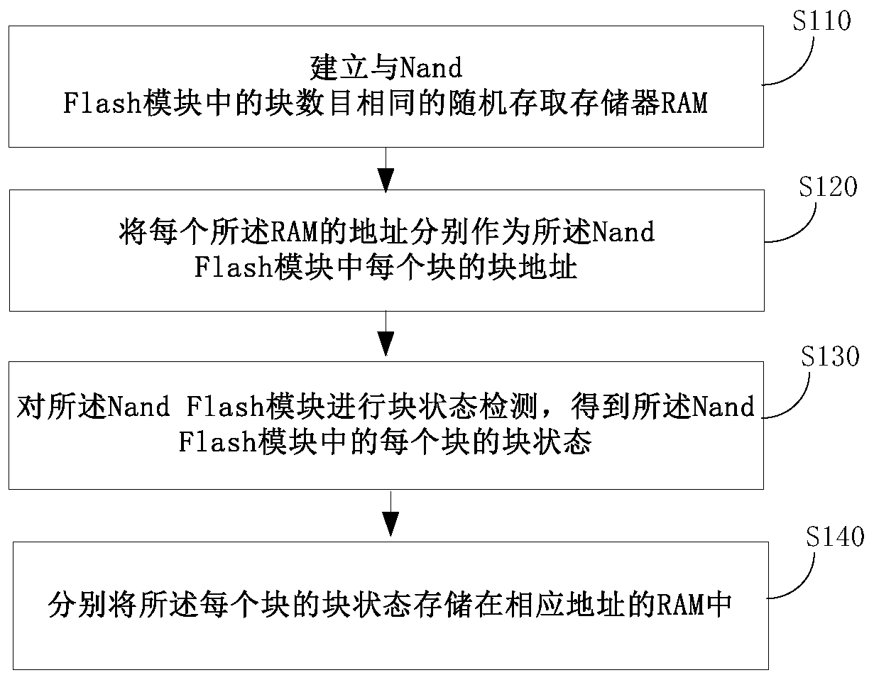
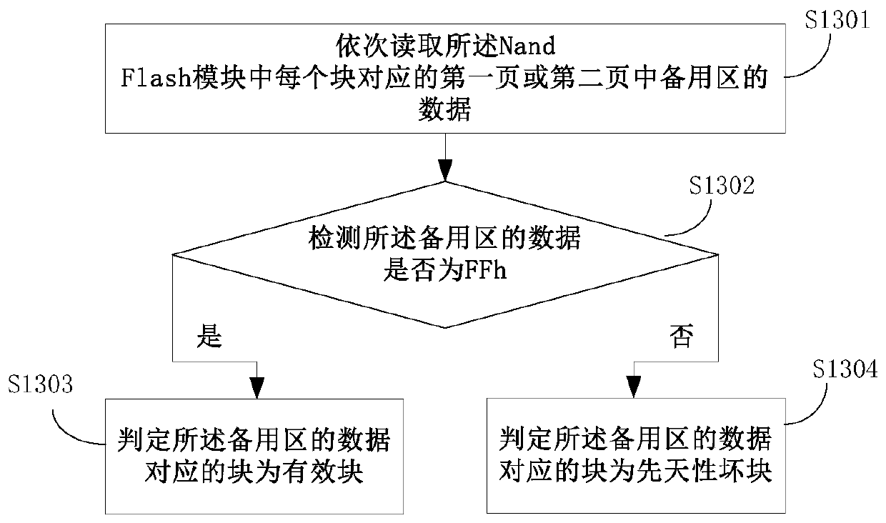
[0062] In the prior art, when the bad blocks in the Nand Flash module are managed, a large amount of FPGA internal RAM resources can be taken up, the embodiment of the invention provides a kind of Nand Flash bad block management method, the core of the method is: Establish the same corresponding RAM space as the number of blocks in the Nand Flash module in the FPGA module, use the address of eac...


PUM


Abstract

The invention discloses a Nand Flash bad block management method and device and a memory. The bad block management method comprises the steps of establishing a random access memory RAM in an FPGA module with the same block number as a Nand Flash module, adopting an address of each RAM as a block address of each block in the Nand Flash module, then, storing a detected block state of the each block in the Nand Flash module into a RAM of the corresponding address so that corresponding writing and reading operation can be conducted according to the address of the each RAM and block state data stored in the RAM. According to the Nand Flash bad block management method and device and the memory, the address of the RAM is adopted as the block address of the each block in the Nand Flash module, and thus the space occupied by the RAM storage block address is saved; moreover, the RAM address needs to be shown with only one counter, thus the storage space of the FPGA module is not occupied, and the inner resource of the FPGA module is further saved.

Description

technical field [0001] The invention relates to the technical field of flash memories, in particular to a Nand Flash bad block management method, device and memory. Background technique [0002] Nand Flash (flash memory) memory is a kind of Flash memory. Because Nand Flash has the advantages of fast data storage speed, large capacity, and many erasable times, it has been more and more widely used in the industry. Since the logic control of NandFlash is relatively complicated, corresponding logic control devices such as microcontrollers, CPLDs (Complex Programmable Logic Devices, complex programmable logic devices), FPGAs (Field Programmable Gate Arrays, Field Programmable Gate Arrays) etc. are required for logic control. Among them, FPGA is widely used because of its high clock frequency, small internal delay and abundant logic resources. [0003] figure 1 It is a schematic diagram of the hardware structure of Nand Flash memory based on FPGA control. like figure 1 As sho...

Claims


Application Information

Patent Timeline
Patent Type & Authority Patents(China)
IPC IPC(8): G06F12/06
CPCG06F12/0646
Inventor 杨艺刘虹兰海洋王耀辉
Owner BEIJING LUSTER LIGHTTECH
Why Eureka
Try Eureka