
Structure and Formation Method of Semiconductor Device Structure

A device structure and semiconductor technology, applied in the direction of semiconductor devices, semiconductor/solid-state device manufacturing, electric solid-state devices, etc., can solve the problems of increasing the complexity of processing and manufacturing IC, and difficult to implement the manufacturing process.

Active Publication Date: 2019-11-22
TAIWAN SEMICON MFG CO LTD
View PDF3 Cites 0 Cited by
  • Summary
  • Abstract
  • Description
  • Claims
  • Application Information

AI Technical Summary

Problems solved by technology

[0004] However, these advances have increased the complexity of handling and manufacturing IC
Manufacturing processes continue to become more difficult due to ever-shrinking component sizes
Therefore, it is a challenge to form reliable semiconductor devices with smaller and smaller dimensions

Method used


Image

  • Structure and Formation Method of Semiconductor Device Structure
  • Structure and Formation Method of Semiconductor Device Structure
  • Structure and Formation Method of Semiconductor Device Structure

Examples


Embodiment Construction

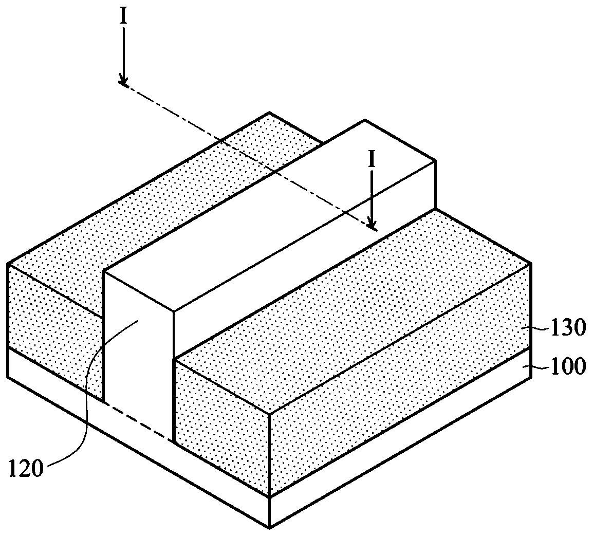
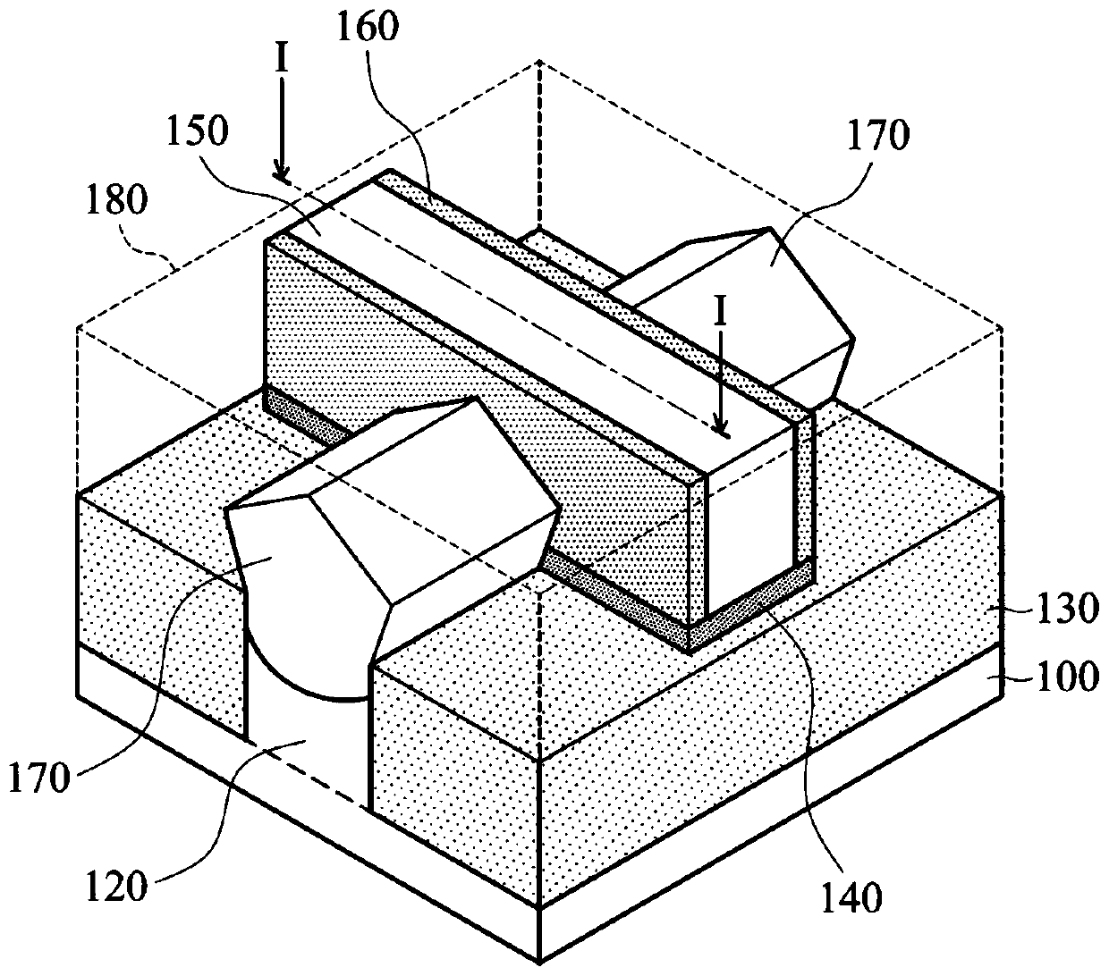
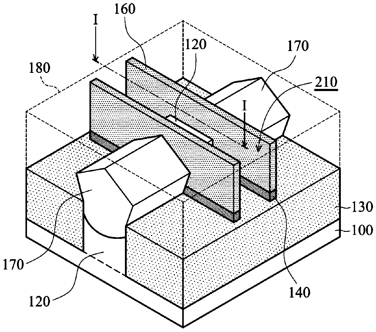
[0012] The following disclosure provides many different embodiments or examples for implementing different features of the presented subject matter. Specific examples of components and arrangements are described below to simplify the present disclosure. Of course, these are examples only and are not intended to limit the invention. For example, in the following description, forming a first component over or on a second component may include embodiments in which the first component and the second component are formed in direct contact, and may also include embodiments where the first component and the second component may be formed in direct contact. Embodiments in which additional components are formed so that the first and second components may not be in direct contact. In addition, the present invention may repeat reference numerals and / or letters in various instances. This repetition is for the sake of simplicity and clarity and does not in itself indicate a relationship ...


PUM


Abstract

Embodiments of the present invention provide structures and methods of forming semiconductor device structures. A semiconductor device structure includes a fin structure over a semiconductor substrate and a gate stack covering a portion of the fin structure. The gate stack includes a gate dielectric layer, a work function layer, and a conductive filler over the work function layer. The semiconductor device structure also includes a dielectric layer covering the fin structure. The dielectric layer is in direct contact with the conductive filler.

Description

technical field [0001] The present invention relates to the field of semiconductors, and more particularly to the structure and formation method of semiconductor device structures. Background technique [0002] The semiconductor integrated circuit (IC) industry has experienced rapid development. Technological advances in IC materials and design have produced generations of ICs. Each generation has smaller and more complex circuits than the previous generation. [0003] During IC evolution, functional density (ie, the number of interconnected devices per chip area) has generally increased while geometry size (ie, the smallest component (or line) that can be created using a fabrication process) has decreased. Such downscaling processes typically provide benefits through increased yield efficiencies and reduced associated costs. [0004] However, these advances have increased the complexity of handling and manufacturing ICs. Manufacturing processes continue to become more d...

Claims


Application Information

Patent Timeline
Patent Type & Authority Patents(China)
IPC IPC(8): H01L29/78H01L21/336
CPCH01L29/66545H01L29/66795H01L29/785H01L29/7848H01L21/28079H01L21/28088H01L21/31051H01L21/32115H01L21/823431H01L27/0886H01L29/4958H01L29/4966H01L29/517H01L29/6681H01L29/7851H01L21/31111H01L29/0649
Inventor 张哲诚林志翰
Owner TAIWAN SEMICON MFG CO LTD
Learn More