PCB test-based processing technology and PCB

A processing technology and PCB board technology, applied in the electronic field, can solve problems such as low test efficiency, large test pin size positioning tolerance, and small testable pad area.

Inactive Publication Date: 2017-05-10
GUANGDONG VTRON TECH CO LTD
View PDF2 Cites 0 Cited by
  • Summary
  • Abstract
  • Description
  • Claims
  • Application Information

AI Technical Summary

Problems solved by technology

[0005] The embodiment of the present invention provides a processing technology and PCB board based on PCB testing, which solves the problem that the current via testable pad area is small, the test pin is deformed or the size positioning tolerance is too large, which leads to test misjudgment and test efficiency. Poor technical issues

Method used


Image

  • PCB test-based processing technology and PCB
  • PCB test-based processing technology and PCB

Examples


Embodiment Construction

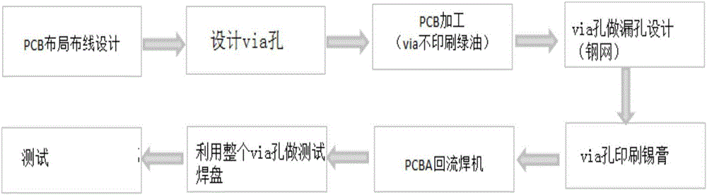
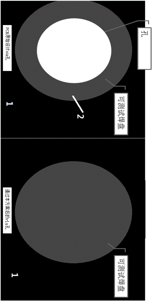
[0028] The embodiment of the present invention provides a processing technology and PCB board based on PCB testing, which solves the problem that the current via testable pad area is small, the test pin is deformed or the size positioning tolerance is too large, which leads to test misjudgment and test efficiency. Poor technical issues.

[0029] In order to make the purpose, features and advantages of the present invention more obvious and understandable, the technical solutions in the embodiments of the present invention will be clearly and completely described below in conjunction with the accompanying drawings in the embodiments of the present invention. Obviously, the following The described embodiments are only some, not all, embodiments of the present invention. Based on the embodiments of the present invention, all other embodiments obtained by persons of ordinary skill in the art without making creative efforts belong to the protection scope of the present invention. ...


PUM


Abstract

The embodiment of the invention discloses a PCB test-based processing technology and a PCB, and aims at solving the technical problems of test misjudgment and low test efficiency caused by a very small testable bonding pad and large test pin deformation or dimension location tolerance of an existing via. The PCB test-based processing technology comprises the steps of determining a via according to a preset PCB layout; carrying out leaking treatment on the via in the processed PCB; and printing solder paste on the via and taking the via as a test bonding pad.

Description

technical field [0001] The invention relates to the field of electronic technology, in particular to a processing technology based on PCB testing and a PCB board. Background technique [0002] Printed circuit board {PCB circuit board}, also known as printed circuit board, is the provider of electrical connections for electronic components. Its development has a history of more than 100 years; its design is mainly layout design; the main advantage of using circuit boards is that it greatly reduces wiring and assembly errors, and improves automation and production labor rates. According to the number of layers of circuit boards, it can be divided into single-sided boards, double-sided boards, four-layer boards, six-layer boards and other multi-layer circuit boards. [0003] Since the printed circuit board is not a general terminal product, the definition of the name is slightly confusing. They are not the same, so when evaluating the industry, the two are related but cannot ...

Claims


Application Information

Patent Timeline
Patent Type & Authority Applications(China)
IPC IPC(8): H05K1/02H05K3/42
CPCH05K1/0268H05K3/42H05K2203/163
Inventor 黄海兵
Owner GUANGDONG VTRON TECH CO LTD
Why Eureka
Try Eureka