Circuit for implementing transistor-level scheme of five-input-end combinational logic circuit

A combination logic circuit, transistor-level technology, applied in logic circuits, logic circuits with logic functions, electrical components, etc., can solve the problems of large transmission delay, large signal transmission delay, large silicon chip area, etc., to reduce the number of transistors. , the effect of silicon wafer area reduction

Inactive Publication Date: 2017-05-17
HEFEI HENGSHUO SEMICON CO LTD
View PDF0 Cites 0 Cited by
  • Summary
  • Abstract
  • Description
  • Claims
  • Application Information

AI Technical Summary

Problems solved by technology

[0005] Second, the signal transmission delay is large
The transmission delay from input to output is too large, and it will be fatal for circuits with high frequency, which are very concerned about the signal delay.
[0007] Third, the required circuit costs are high
[0008] Since the existing circuit uses 2 inverter

Method used


Image

  • Circuit for implementing transistor-level scheme of five-input-end combinational logic circuit
  • Circuit for implementing transistor-level scheme of five-input-end combinational logic circuit

Examples


Example Embodiment

[0016] Hereinafter, preferred embodiments of the present invention are given in conjunction with the drawings to illustrate the technical solutions of the present invention in detail.

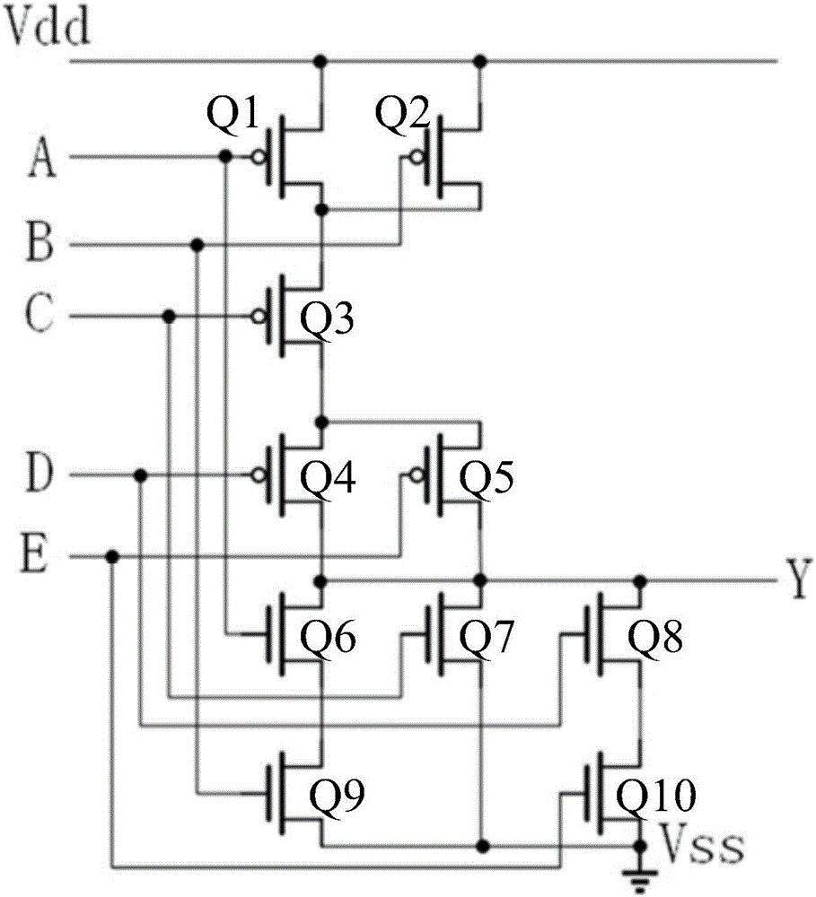
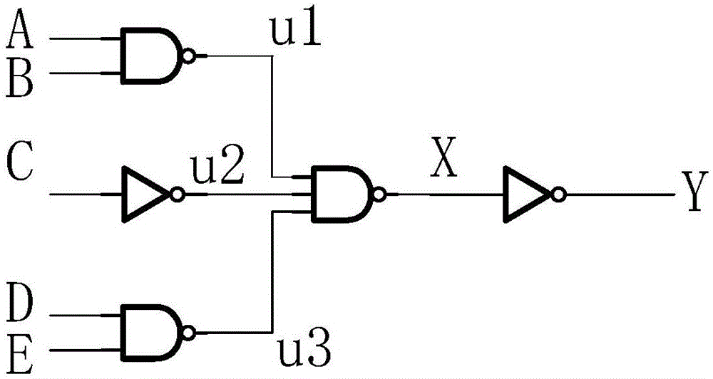
[0017] Such as figure 1 As shown, the circuit of the transistor-level implementation scheme of the five-input combinational logic circuit of the present invention includes a first triode Q1, a second triode Q2, a third triode Q3, a fourth triode Q4, and a fifth triode. The transistor Q5, the sixth transistor Q6, the seventh transistor Q7, the eighth transistor Q8, the ninth transistor Q9, the thirteenth transistor Q10, the drain of the first transistor Q1 and the third The drain of the second transistor Q2 is connected, the gate of the first transistor Q1 is connected to the gate of the sixth transistor Q6, the source of the first transistor Q1 and the drain of the third transistor Q3 Connected, the gate of the second transistor Q2 is connected to the gate of the ninth transistor Q9, the source ...


PUM


Abstract

The invention discloses a circuit for implementing a transistor-level scheme of a five-input-end combinational logic circuit. The circuit comprises a first triode, a second triode, a third triode, a fourth triode, a fifth triode, a sixth triode, a seventh triode and the like, wherein a drain electrode of the first triode is connected with a drain electrode of the second triode, a grid electrode of the first triode is connected with a grid electrode of the sixth triode, a source electrode of the first triode is connected with a drain electrode of the third triode, a grid electrode of the second triode is connected with a grid electrode of a ninth triode, a source electrode of the second triode is connected with the drain electrode of the third triode, a source electrode of the third triode is connected with a drain electrode of the fourth triode, a grid electrode of the fourth triode is connected with a grid electrode of an eighth triode, and a source electrode of the fourth triode is connected with a drain electrode of the sixth triode. The circuit has the advantage that the number of transistors is decreased, so that the silicon wafer area occupied by same logic functions is reduced substantially.

Description

technical field [0001] The invention relates to a combinational logic circuit, in particular to a circuit of a transistor-level realization scheme of a five-input terminal combinational logic circuit. Background technique [0002] There are the following disadvantages and deficiencies in the current circuit for implementing the transistor-level implementation scheme of the five-input combinational logic circuit in the prior art: [0003] First, the circuit is complex and requires a large number of logic gates [0004] Prior art needs to realize logic Y=~((A·B)+C+(D·E)), compiled by hardware description language Verilog code, then after synthesis, it will be as follows figure 2 Shown: Called 2 inverters, 1 3-input NAND gate and 2 2-input NAND gates. [0005] Second, the signal transmission delay is large [0006] When the signal is transmitted through the three-level gate, due to the inherent delay of the gate itself, the total transmission delay from input to output incre...

Claims


Application Information

Patent Timeline
IPC IPC(8): H03K19/20H03K19/0944
CPCH03K19/0944H03K19/20
Inventor 唐立伟任军
Owner HEFEI HENGSHUO SEMICON CO LTD
Why Eureka
Try Eureka