Display substrate, display device and driving method of display device

A technology for display substrates and display devices, applied in static indicators, instruments, semiconductor devices, etc., can solve the problems of increasing the number of gate drive chips, reducing the aperture ratio, and disadvantageous narrow borders, etc., to improve display quality and improve aperture ratio. , the effect of improving the pixel charging rate

Active Publication Date: 2017-05-24
BOE TECH GRP CO LTD +1
View PDF4 Cites 19 Cited by
  • Summary
  • Abstract
  • Description
  • Claims
  • Application Information

AI Technical Summary

Problems solved by technology

However, although two adjacent gate lines give the same timing, they are two independent gate lines in the design. Since the gate lines occupy a certain space, the pixel opening area is compressed and the aperture ratio is reduced.
At the same time, the number of gate lines is large, which leads to an increase in the number of gate drive chips, an increase in cost, and is not conducive to the realization of narrow borders.

Method used


Image

  • Display substrate, display device and driving method of display device
  • Display substrate, display device and driving method of display device
  • Display substrate, display device and driving method of display device

Examples


Embodiment 1

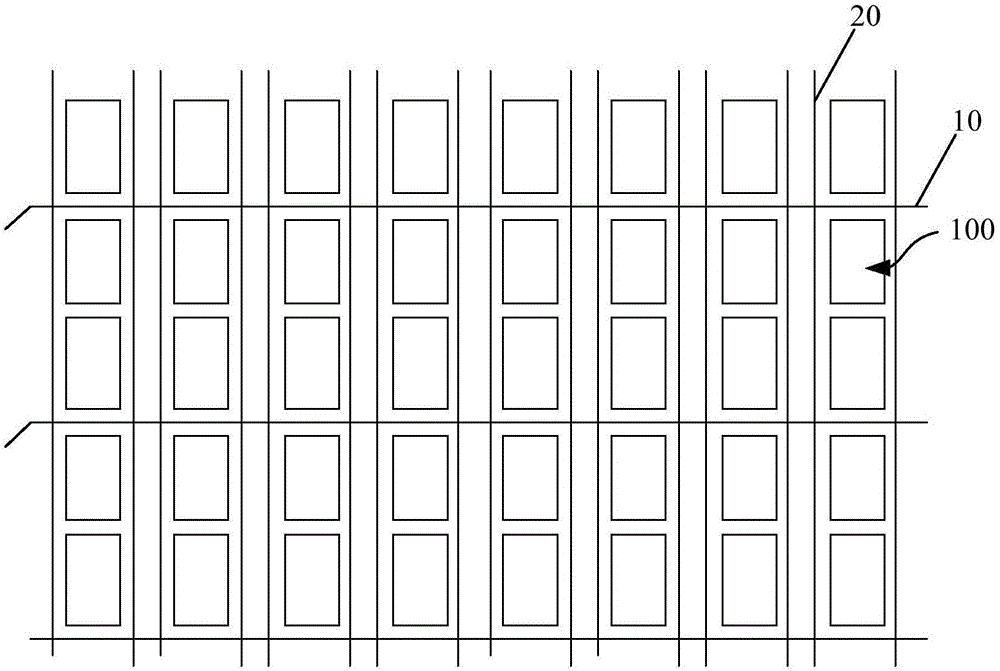
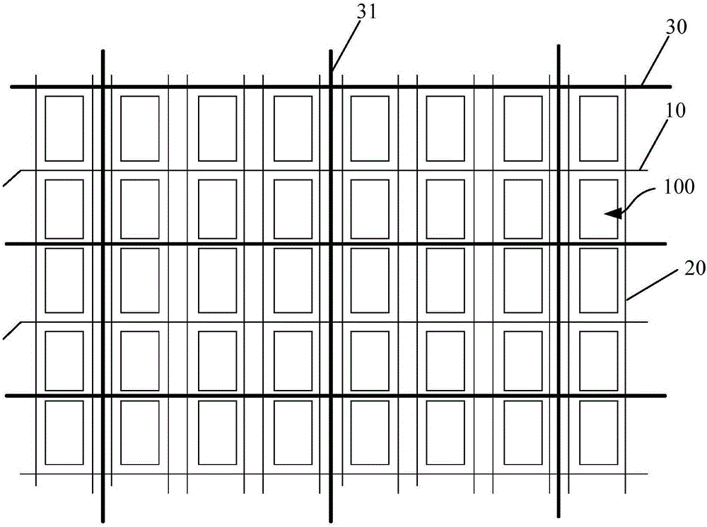
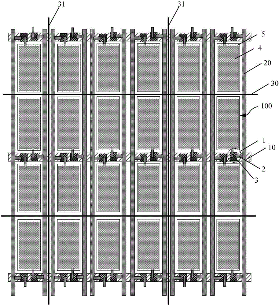
[0021] to combine figure 1 and image 3 As shown, in this embodiment, a display substrate is provided, including a plurality of gate lines 10 and a plurality of data lines 20 , and the gate lines 10 and data lines 20 are distributed across and define a plurality of sub-pixel regions 100 . There are two rows of sub-pixel regions 100 between two adjacent gate lines 10 , and two data lines 20 between two adjacent columns of sub-pixel regions 100 . Each sub-pixel region 100 includes a thin film transistor 1 , the gate electrode of the thin film transistor 1 is integrally formed with the gate line 10 , the source electrode 2 is connected to the data line 20 , and the corresponding thin film transistor 1 is turned on or off through the gate line 10 .

[0022] The thin film transistors 1 of two adjacent rows of sub-pixel regions 100 located on both sides of a gate line 10 are connected to the gate line 10, and the thin film transistors 1 of adjacent two rows of sub-pixel regions loc...

Embodiment 2

[0049] This embodiment provides a display device and a driving method thereof. The display device adopts the display substrate in the first embodiment, and since the number of gate lines is halved, the aperture ratio is increased. At the same time, halving the number of gate lines reduces the number of gate drive chips or gate drive circuits, reduces costs, and facilitates the realization of narrow borders. In addition, since the thin film transistors in one row of sub-pixel regions can open the charging time of two rows of sub-pixels, sufficient charging time is provided, thereby increasing the pixel charging rate and improving display quality.

[0050] Wherein, the display device may be a liquid crystal display device, an organic electroluminescent display device, or the like.

[0051] The driving method of the above display device includes:

[0052] The thin film transistors in two adjacent rows of sub-pixel regions located on both sides of the gate line are simultaneousl...


PUM


Abstract

The invention relates to the technical field of displaying and discloses a display substrate, a display device and a driving method of the display device; two rows of sub-pixel areas are arranged between every two adjacent gate lines of the display substrate, the adjacent rows of sub-pixel areas on two sides of each gate line share one gate line, so that the gate lines are halved, pixel aperture areas are increased and aperture rate is increased; in addition, as the gate lines are halved, the number of gate drive chips or gate drive circuits is decreased, the cost is lowered and a narrow bezel is achieved; in addition, the charge time of one row of sub-pixel area is doubled, sufficient charge time is provided, and accordingly, pixel charging rate is increased and displaying quality is improved.

Description

technical field [0001] The present invention relates to the field of display technology, in particular to a display substrate, a display device and a driving method thereof. Background technique [0002] In the field of flat panel display technology, thin film transistors (Thin Film Transistor, TFT for short) have the advantages of small size, low power consumption, and relatively low manufacturing cost, and are widely used as driving devices in flat panel display technology. [0003] For a TFT display device, the TFT is controlled to be turned on or off through the gate line, and when the TFT is turned on, the pixel voltage is transmitted to the corresponding pixel through the data line. The pixel charging rate is defined as the ratio of the pixel voltage of the pixel to the voltage written on the data line. The pixel voltage is related to charging time, TFT turn-on current, etc. Taking a 120Hz display device (with a resolution of 3840*2160) as an example, the charging ti...

Claims


Application Information

Patent Timeline
Patent Type & Authority Applications(China)
IPC IPC(8): G02F1/1362G02F1/1368G02F1/133
CPCG02F1/13306G02F1/136286G02F1/1368G02F2201/40H01L27/124G02F1/134363G02F2201/121G09G3/3607G09G3/3614G09G3/3688
Inventor 戴珂江鹏
Owner BOE TECH GRP CO LTD
Why Eureka
Try Eureka