A kind of fpga chip wiring method

A wiring method and wiring technology, applied in the direction of instruments, calculations, electrical digital data processing, etc., can solve the problem of not increasing the wiring speed, and achieve the effect of reducing time delay and improving wiring speed

Active Publication Date: 2021-05-07
CAPITAL MICROELECTRONICS
View PDF3 Cites 0 Cited by
  • Summary
  • Abstract
  • Description
  • Claims
  • Application Information

AI Technical Summary

Problems solved by technology

[0004] With the expansion of the scale of FPGA chips, the requirements for wiring speed are getting higher and higher. At present, the industry has not provided a method to improve the wiring speed.

Method used


Image

  • A kind of fpga chip wiring method
  • A kind of fpga chip wiring method
  • A kind of fpga chip wiring method

Examples


Embodiment Construction

[0018]In order to make the objects, technical solutions, and advantages of the present invention more clearly, the technical solutions in the embodiments of the present invention will be described in contemplation in the embodiments of the present invention, and will be described, and the embodiments described in the embodiments of the present invention will be described. It is a part of the embodiments of the present invention, not all of the embodiments.

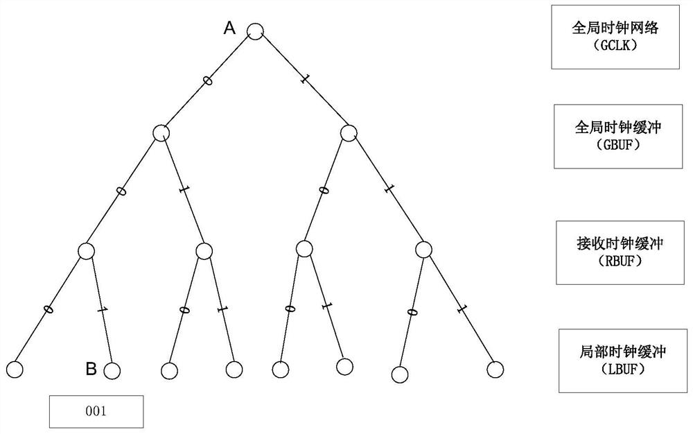
[0019]The embodiment of the present invention provides an FPGA chip wiring method, which analyzes the wiring module characteristics of the FPGA chip architecture to improve the wiring speed and reduce the delay of the time.

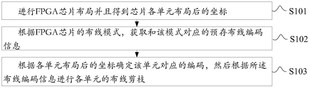
[0020]figure 1 A method of fpga chip wiring method according to an embodiment of the present invention is shown. Such asfigure 1 As shown, an FPGA chip wiring method includes steps S101-S103:

[0021]Step S101: Perform the FPGA chip layout and obtain coordinates after the layout of each unit of the chip;

[0022]Specif...


PUM


Abstract

The invention relates to an FPGA chip wiring method, the method comprising: performing FPGA chip layout and obtaining the coordinates of each unit layout of the chip; according to the wiring mode of the FPGA chip, obtaining pre-stored wiring coding information corresponding to the mode; according to the layout of each unit The final coordinates determine the code corresponding to the unit, and then perform wiring pruning for each unit according to the wiring code information. The invention obtains the wiring coding information of the wiring pattern in the FPGA chip, and then performs reasonable pruning in the actual wiring process according to the pre-stored wiring coding information, thereby increasing the wiring speed and reducing the time delay.

Description

Technical field[0001]The present invention relates to the field of integrated circuit design in the field of microelectronics, particularly an FPGA chip wiring method.Background technique[0002]FPGA is a logic device with enriching hardware resources, powerful parallel processing capabilities, and flexible and heavy configurable. These features have enabled FPGA to have more and more widely used in many fields such as data processing, communication, and networks.[0003]Currently, in the Field Programmable Gate Array, FPGA applications, the integrated circuit requires a programmable or configurable interconnect network, and the logic gate is connected to each other by a configurable interconnection network. FPGAs that act as a core part of a stand-alone chip or system have been widely used in a large number of microelectronic devices. The definition of the logic door of a broad FPGA, not only simple and non-door, also refers to a logic unit (LE, Logic Element) having a combination logi...

Claims


Application Information

Patent Timeline
Patent Type & Authority Patents(China)
IPC IPC(8): G06F30/347
CPCG06F30/392
Inventor 刘桂林
Owner CAPITAL MICROELECTRONICS
Why Eureka
Try Eureka