Array substrate, display panel and display device

A technology for an array substrate and a display panel is applied in the fields of display panels, display devices, and array substrates, and can solve problems such as damage to the array substrate, and achieve the effects of enhancing strength, avoiding damage, and improving cutting yield.

Active Publication Date: 2017-05-24
BOE TECH GRP CO LTD +1
View PDF3 Cites 7 Cited by
  • Summary
  • Abstract
  • Description
  • Claims
  • Application Information

AI Technical Summary

Problems solved by technology

[0004] The present invention aims at the above-mentioned deficiencies in the prior art, and provides an array substrate, a display panel and a display device, which are used to at least partially solve the problem that the array substrate is easily damaged during the cutting process

Method used


Image

  • Array substrate, display panel and display device
  • Array substrate, display panel and display device
  • Array substrate, display panel and display device

Examples


Embodiment Construction

[0028] The technical solutions in the present invention will be clearly and completely described below in conjunction with the accompanying drawings in the present invention. Apparently, the described embodiments are part of the embodiments of the present invention, not all of them. Based on the embodiments of the present invention, all other embodiments obtained by persons of ordinary skill in the art without making creative efforts belong to the protection scope of the present invention.

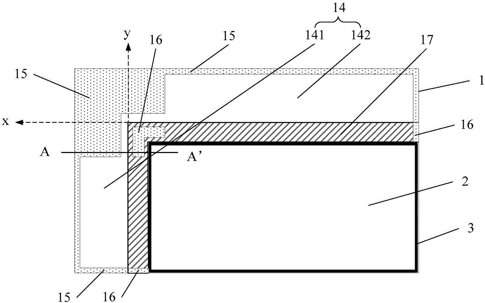
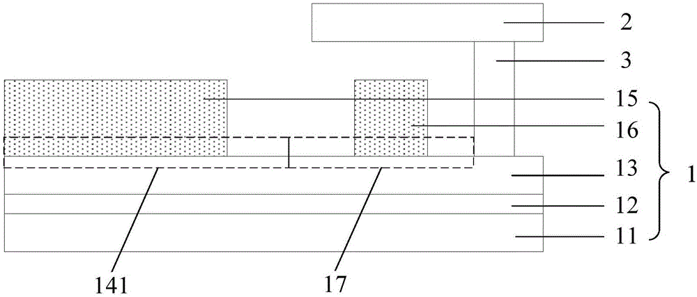
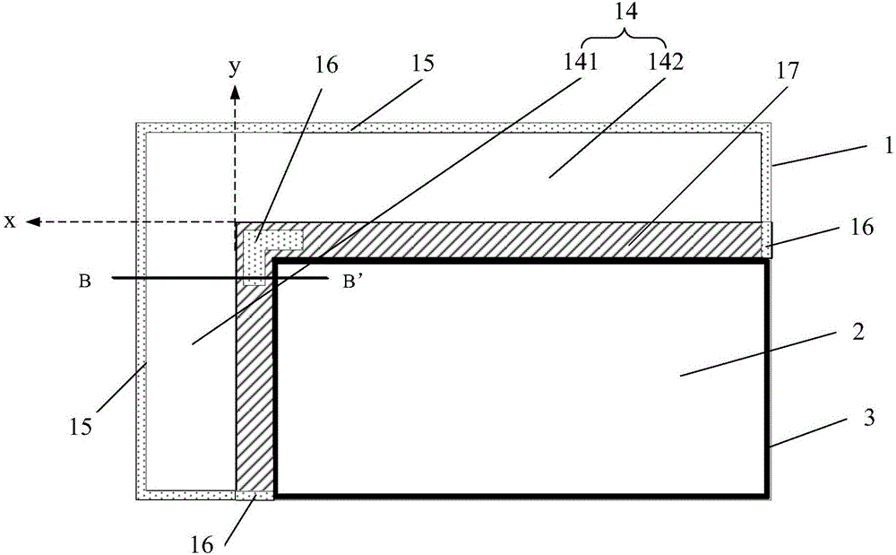
[0029] combine Figure 1a , Figure 1b , Figure 2a and Figure 2b As shown, the embodiment of the present invention provides an array substrate 1 , and the array substrate includes a wiring 12 and an insulating layer 13 sequentially formed on a base substrate 11 . The wires 12 may be metal wires such as gate wires, data wires, and test wires, and the insulating layer 13 covers the wires 12 to play the role of insulation and protection. The side of the insulating layer 13 of the array s...


PUM


Abstract

The invention provides an array substrate, a display panel and a display device. The array substrate comprises a line and an insulating layer, wherein the line and the insulating layer are sequentially formed on a liner substrate; a binding area is arranged at one side far away from the line, of the insulating layer of the array substrate; a first protection layer which is at least partially parallel to the edge of the array substrate is arranged inside the binding area of the array substrate. In the process that the array substrate is cut, the first protection layer has a support function for the liner substrate to a certain extent, the strength of the liner substrate can be improved, the liner substrate can be prevented from damage, and thus the cutting pass percent can be increased.

Description

technical field [0001] The present invention relates to the field of display technology, in particular to an array substrate, a display panel and a display device. Background technique [0002] During the manufacturing process of the display panel, the array substrate is usually larger than the color filter substrate in the length direction and width direction due to the arrangement of electrodes and metal wiring, etc., and the area on the array substrate that does not correspond to the color filter substrate is the bound area. [0003] When cutting the array substrate, since the base substrate at the binding area of ​​the array substrate is a single piece of glass (the color filter substrate does not extend above it), the base substrate at the corner of the binding area of ​​the array substrate Shell-shaped damage often occurs. When the base substrate has burrs, it needs to be polished, but due to the insufficient strength of the base substrate, it is also prone to damage ...

Claims


Application Information

Patent Timeline
Patent Type & Authority Applications(China)
IPC IPC(8): H01L27/12
CPCH01L27/1214H01L27/1218G02F1/133351G02F2201/50G02F1/1303G02F1/1333G02F1/133354G02F1/133388H01L27/1244H01L27/1288H05B33/04G02F1/133331
Inventor 刘利萍黄静陈仁坦
Owner BOE TECH GRP CO LTD
Why Eureka
Try Eureka