Semiconductor radiation detector based on Bi-based quaternary halide single crystal, and manufacturing method thereof

A technology of radiation detectors and semiconductors, applied in semiconductor devices, electrical components, circuits, etc., can solve problems such as poor stability, environmental pollution, and low sensitivity

Active Publication Date: 2017-05-24
HUAZHONG UNIV OF SCI & TECH
View PDF3 Cites 18 Cited by
  • Summary
  • Abstract
  • Description
  • Claims
  • Application Information

AI Technical Summary

Problems solved by technology

[0004] The present invention proposes a semiconductor radiation detector based on a Bi-based quaternary halide single crystal and a preparation method, the purpose of which is to obtain a high-performance, non-toxic and stable semiconductor radiation detector, and to solve the complex process and low sensitivity of the prior art , environmental pollution and poor stability, and indicators such as sensitivity, working bias voltage, stability and environmental pollution cannot take into account the problem

Method used


Image

  • Semiconductor radiation detector based on Bi-based quaternary halide single crystal, and manufacturing method thereof
  • Semiconductor radiation detector based on Bi-based quaternary halide single crystal, and manufacturing method thereof
  • Semiconductor radiation detector based on Bi-based quaternary halide single crystal, and manufacturing method thereof

Examples


Embodiment example 1

[0036] This example will introduce cesium silver bismuth bromide (Cs 2 AgBr 6 ) preparation of the crystal and the preparation of the semiconductor radiation detector with the crystal:

[0037] Take silver bromide (AgBr, 0.188g, 1mmol), bismuth bromide (BiBr 3 , 0.449g, 1mmol) and cesium bromide (CsBr, 0.426g, 2mmol) were added to 10ml of hydrobromic acid (HBr) solution, the solution was heated to 130°C to fully dissolve the solution, and then 1°C / h The speed is lowered to 60 ° C, and crystals are precipitated, thereby obtaining cesium silver bismuth bromide (Cs 2 AgBr 6 ) crystals.

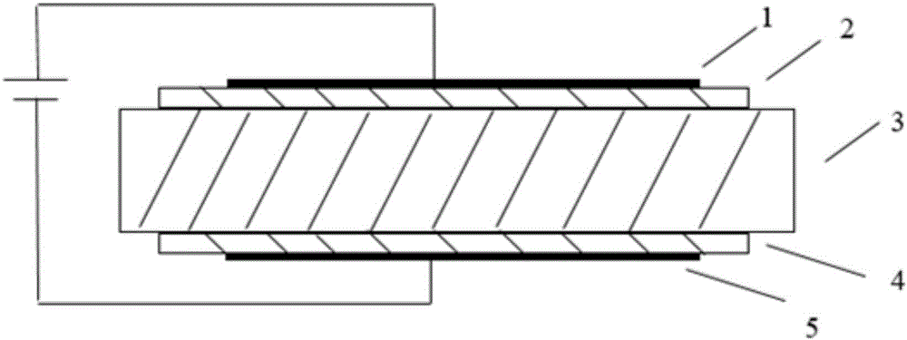
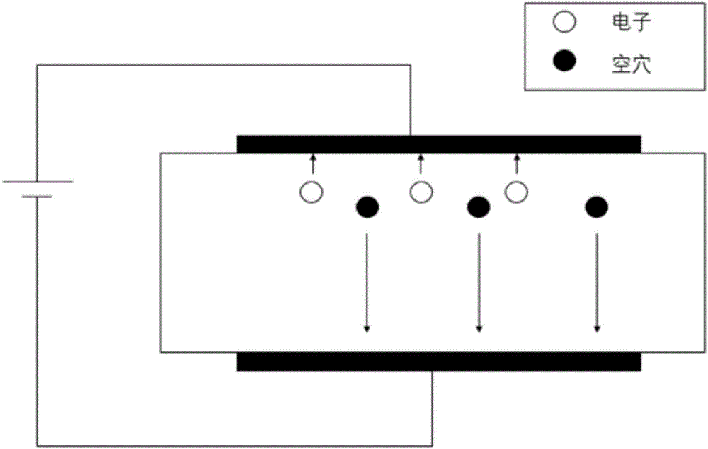
[0038] A gold electrode with a thickness of 80 nm was evaporated on the upper and lower surfaces of the crystal by thermal evaporation.

Embodiment example 2

[0040] This example will introduce cesium silver bismuth bromide (Cs 2 AgBr 6 ) crystal, and add charge selective contact layer on this crystal to prepare semiconductor radiation detector:

[0041] Take silver bromide (AgBr, 0.188g, 1mmol), bismuth bromide (BiBr 3 , 0.449g, 1mmol) and cesium bromide (CsBr, 0.426g, 2mmol) were added to 10ml of hydrobromic acid (HBr) solution, the solution was heated to 130°C to fully dissolve the solution, and then 1°C / h The speed is lowered to 60 ° C, and crystals are precipitated, thereby obtaining cesium silver bismuth bromide (Cs 2 AgBr 6 ) crystals.

[0042] On the upper surface of the crystal, carbon sixty (C 60 ).

[0043] A gold electrode with a thickness of 80 nm was evaporated on the upper and lower surfaces of the crystal by thermal evaporation.

Embodiment example 3

[0045] This example will introduce cesium silver bismuth chloride (Cs 2 AgBiCl 6 ) preparation of the crystal and the preparation of the semiconductor radiation detector with the crystal:

[0046] Take silver chloride (AgCl, 0.144g, 1mmol), bismuth chloride (BiBr 3 , 0.317g, 1mmol) and cesium chloride (CsCl, 0.382g, 2mmol) were added to 10ml of hydrochloric acid (HCl) solution, the solution was heated to 120°C to fully dissolve the solution, and then at a rate of 0.5°C / h The temperature is lowered to 60°C, and crystals are precipitated to obtain cesium silver bismuth chloride (Cs 2 AgBiCl 6 ) crystals.

[0047] A gold electrode with a thickness of 80 nm was evaporated on the upper and lower surfaces of the crystal by thermal evaporation.

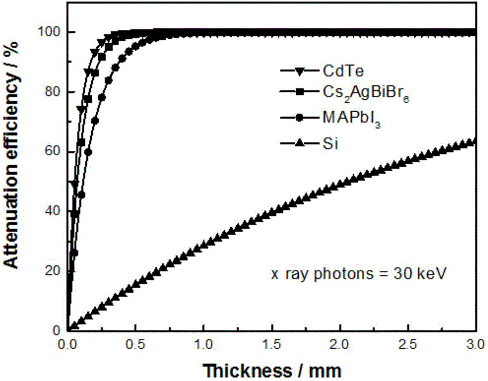
[0048] It can be seen from the examples that the semiconductor radiation detector prepared by the present invention has the advantages of high sensitivity, stability, and environmental friendliness.


PUM


Abstract

The invention discloses a semiconductor radiation detector based on a Bi-based quaternary halide single crystal, and a manufacturing method of the semiconductor radiation detector, which relate to the technical field of ray imaging detectors manufactured by a semiconducting material. The semiconductor radiation detector comprises the Bi-based quaternary halide single crystal serving as a ray absorption layer, an electron selective contact layer and a hole selective contact layer, wherein the electron selective contact selection layer and the hole selective contact layer are adhered to two surfaces of the ray absorption layer separately, and two electrodes are in contact with the two selective charge contact layers separately and serve as a positive electrode and a negative electrode of the device. The semiconductor radiation detector has the advantages of high sensitivity, environment friendliness, stability and the like.

Description

technical field [0001] The invention belongs to the technical field of radiation imaging detectors made of semiconductor materials, and more specifically relates to an imaging detector and a preparation method for preparing X-rays and Gama rays by using Bi-based quaternary halide single crystals. Background technique [0002] Radiographic imaging technology uses radioactive rays (such as X-rays and γ-rays, etc.) as a medium to obtain structural or functional information of the detected object in the form of images, and provides various technologies for diagnosing, detecting and monitoring the observed objects for the corresponding industries. It is widely used in industries such as medical and health care, public safety and high-end manufacturing. Detectors are an important part of radiography equipment. Detectors used to detect radioactive rays generally include gas detectors, scintillation detectors, semiconductor detectors, etc., among which semiconductor detectors can o...

Claims


Application Information

Patent Timeline
Patent Type & Authority Applications(China)
IPC IPC(8): H01L31/10H01L31/18H01L31/032
CPCH01L31/032H01L31/022408H01L31/115H01L31/18H01L31/10
Inventor 唐江潘伟程巫皓迪罗佳俊牛广达周英
Owner HUAZHONG UNIV OF SCI & TECH
Why Eureka
Try Eureka