Polysilicon thin film processing method, thin film transistor, array substrate and display panel

A polysilicon thin film and thin film transistor technology, which is applied in the manufacture of transistors, semiconductor devices, semiconductor/solid state devices, etc., can solve the problems of polysilicon thin film surface roughness, tip discharge, leakage current, etc., to avoid tip discharge phenomenon, large Leakage current, effect of improving product quality

Active Publication Date: 2020-01-03
WUHAN CHINA STAR OPTOELECTRONICS TECH CO LTD
View PDF6 Cites 0 Cited by
  • Summary
  • Abstract
  • Description
  • Claims
  • Application Information

AI Technical Summary

Problems solved by technology

[0004] The present invention mainly provides a method for preparing a low-temperature polysilicon film, a thin film transistor, an array substrate, and a display panel, aiming to solve the problem of tip discharge and leakage current caused by the high surface roughness of the polysilicon film

Method used


Image

  • Polysilicon thin film processing method, thin film transistor, array substrate and display panel
  • Polysilicon thin film processing method, thin film transistor, array substrate and display panel
  • Polysilicon thin film processing method, thin film transistor, array substrate and display panel

Examples


Embodiment Construction

[0021] In order for those skilled in the art to better understand the technical solution of the present invention, a polysilicon thin film processing method, thin film transistor, array substrate and display panel provided by the present invention will be further described in detail below with reference to the accompanying drawings and specific embodiments.

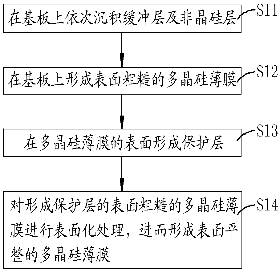
[0022] Please also refer to figure 1 and figure 2 , the polysilicon film processing method embodiment provided by the present invention comprises:

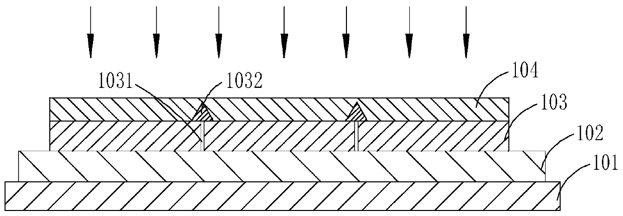
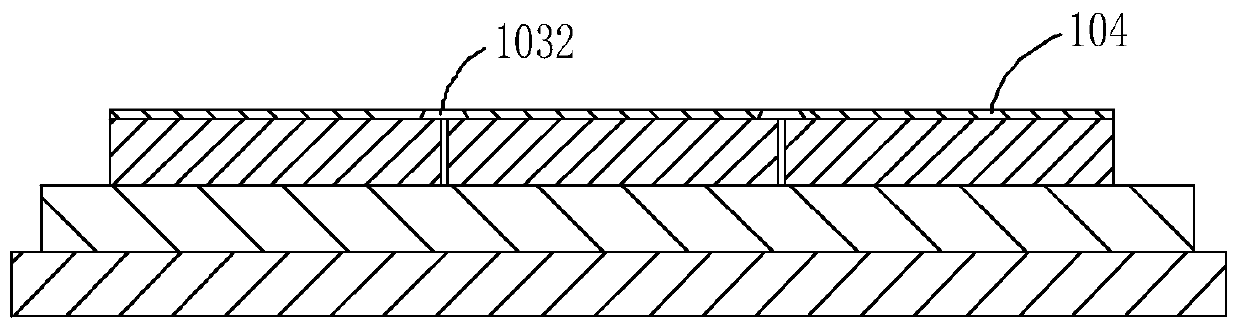
[0023] S11: sequentially depositing a buffer layer 102 and an amorphous silicon layer 103 on the substrate 101;

[0024] Specifically, the buffer layer 102 and the amorphous silicon layer 103 can be sequentially deposited on the substrate 101 by methods including but not limited to plasma enhanced chemical vapor deposition, sputtering, vacuum plating and low pressure chemical vapor deposition.

[0025] Wherein, the buffer layer 102 may be a double-layer structure including...


PUM

PropertyMeasurementUnit
thicknessaaaaaaaaaa
thicknessaaaaaaaaaa
Overlap degreeaaaaaaaaaa

Abstract

The invention provides a polycrystalline silicon thin film processing method, a thin film transistor, an array substrate and a display panel. The method comprises the following steps: forming a polycrystalline silicon thin film with a coarse surface on a substrate; forming a protective layer on the surface of the polycrystalline silicon thin film; carrying out surface processing on the polycrystalline silicon thin film with the coarse surface on which the protective layer is formed, and then forming a polycrystalline silicon thin film with a smooth surface. Through the method, the polycrystalline silicon thin film with the smooth surface can be formed, and then relatively large leakage current generated by a point discharge phenomenon caused by the coarse polycrystalline silicon thin film is avoided in the corresponding array substrate and display panel, so that the product quality is improved.

Description

technical field [0001] The invention relates to the technical field of display panels, in particular to a polysilicon thin film processing method, a thin film transistor, an array substrate and a display panel. Background technique [0002] The electron mobility of amorphous silicon is low, while low-temperature polysilicon can be produced at low temperature, and the electron mobility of low-temperature polysilicon is 20-100 times higher than that of amorphous silicon, so it is suitable for high-resolution small-size displays . However, because the density of molten silicon is higher than that of solid silicon, when using excimer laser annealing method to prepare low-temperature polysilicon, during the crystallization process, excess molten silicon will crystallize at the grain boundary, forming The height of the surface protrusions can reach 10-20nm, which makes the surface roughness of low-temperature polysilicon high. However, in a general polysilicon thin film transist...

Claims


Application Information

Patent Timeline
Patent Type & Authority Patents(China)
IPC IPC(8): H01L21/3065H01L21/306H01L29/786
CPCH01L21/30604H01L21/3065H01L29/78672
Inventor 王威梁博
Owner WUHAN CHINA STAR OPTOELECTRONICS TECH CO LTD
Why Eureka
Try Eureka