Solid-state plasma PiN diode and preparation method therefor

A plasma and diode technology, applied in semiconductor/solid-state device manufacturing, semiconductor devices, electrical components, etc., to achieve the effect of increasing breakdown voltage and enhancing controllability

Active Publication Date: 2017-05-31
XIDIAN UNIV
View PDF2 Cites 2 Cited by
  • Summary
  • Abstract
  • Description
  • Claims
  • Application Information

AI Technical Summary

Benefits of technology

The technical feature described in this patented technology relates to improving the control over the dopants distributed within a semiconductive material called pnictogenesis (PN) region during fabricating electronic devices such as integrated circuits or radio frequency identification tags. By utilizing specific techniques like chemical vapor deposition (CVD), ion beam sputtering, atomic layer epitaxy, etc., these methods allow precise placement of different materials onto desired areas without causing damage. Additionally, they improve the efficiency of producing highly uniform films while also enhancing their properties. Overall, these improvements help create more reliable and efficient electronics products.

Problems solved by technology

This patented technical problem addressed in this patents relates to developing an improved type of small device called Plasma Antenna, specifically designed to overcome issues such as rigidity and lack flexibility caused by previous designs.

Method used


Image

  • Solid-state plasma PiN diode and preparation method therefor
  • Solid-state plasma PiN diode and preparation method therefor
  • Solid-state plasma PiN diode and preparation method therefor

Examples


Embodiment 1

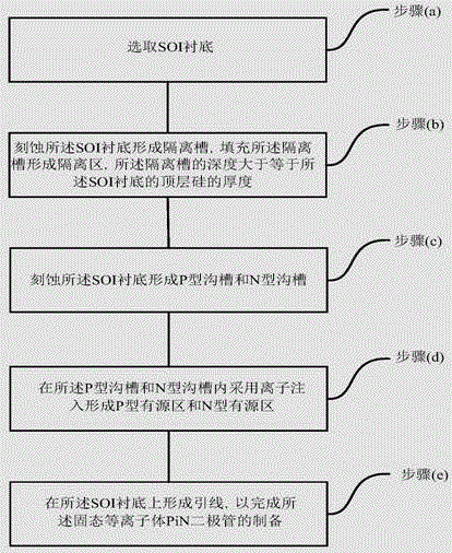
[0064] See figure 1 , figure 1 It is a flow chart of a method for manufacturing a solid-state plasma PiN diode according to an embodiment of the present invention. The method is suitable for preparing a SOI-based lateral solid-state plasma PiN diode, and the SOI lateral solid-state plasma PiN diode is mainly used for manufacturing a solid-state plasma antenna. The method comprises the steps of:

[0065] (a) Select the SOI substrate.

[0066] (b) Etching the SOI substrate to form an isolation groove, filling the isolation groove to form an isolation region, and the depth of the isolation groove is greater than or equal to the thickness of the top layer silicon of the SOI substrate.

[0067] (c) etching the SOI substrate to form a P-type trench and an N-type trench;

[0068] (d) forming a P-type active region and an N-type active region by ion implantation in the P-type trench and the N-type trench; and

[0069] (e) Leads are formed on the SOI substrate to complete the fabri...

Embodiment 2

[0101] See Figure 2a-Figure 2s , Figure 2a-Figure 2s It is a schematic diagram of a method for preparing a solid-state plasma PiN diode according to an embodiment of the present invention. On the basis of the first embodiment above, it will be described in detail by taking the preparation of an SOI-based solid-state plasma PiN diode with a solid-state plasma region length of 100 microns as an example. Specific steps are as follows:

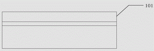
[0102] S10, selecting an SOI substrate.

[0103] See Figure 2a , the crystal orientation of the SOI substrate 101 may be (100) or (110) or (111), and there is no limitation here. In addition, the doping type of the SOI substrate 101 may be n-type or p-type, the doping concentration is, for example, 10 14 ~10 15 cm -3 That is, the resistivity is 40-1000 Ω·cm, and the thickness of the top layer Si is, for example, 0.5-80 μm.

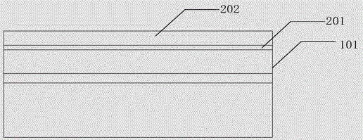
[0104] S20, forming a first protection layer on the SOI substrate.

[0105] See Figure 2b , two layers of mater...

Embodiment 3

[0141] Please refer to image 3 , image 3 It is a schematic diagram of a device structure of a solid-state plasma PiN diode according to an embodiment of the present invention. The solid-state plasmonic PiN diode employs the above-mentioned as figure 1prepared as indicated. Specifically, the solid-state plasma PiN diode is prepared and formed on the SOI substrate 301, and the P region 305, the N region 306 of the pin diode, and the I region laterally located between the P region 305 and the N region 306 are all located on the SOI substrate. within the top layer of silicon 302 of the substrate. Wherein, the pin diode can be isolated by STI deep trenches, that is, an isolation trench 303 is provided outside the P region 305 and the N region 306 , and the depth of the isolation trench 303 is at least greater than or equal to the thickness of the top layer silicon 302 . In addition, the P region 305 and the N region 306 may respectively include a thin-layer P-type active regi...


PUM

PropertyMeasurementUnit
Lengthaaaaaaaaaa
Resistivityaaaaaaaaaa
Thicknessaaaaaaaaaa

Abstract

The invention relates to a solid-state plasma PiN diode and a preparation method therefor. The preparation method comprises the steps of selecting an SOI substrate; etching the SOI substrate to form an isolation groove; filling the isolation groove to form an isolation region, wherein the depth of the isolation groove is greater than or equal to the thickness of top layer silicon of the SOI substrate; etching the SOI substrate to form a P type trench and an N type trench; performing ion implantation in the P type trench and the N type trench to form a P type active region and an N type active region; and forming leads on the SOI substrate to complete the preparation of the solid-state plasma PiN diode. According to the embodiments, the high-performance solid-state plasma PiN diode, which is applicable to formation of a solid-state plasma antenna, can be prepared and provided through a deep trench isolation technology and an ion implantation process.

Description


Claims


Application Information

Patent Timeline
Owner XIDIAN UNIV
Why Eureka
Try Eureka